1 Introduction
This article refers to the address: http://
With the development of deep sub-micron technology, the scale of digital circuits has grown to millions or even tens of millions. The process is also increased from tens of μm to 65 nm or even 45 nm. The timing of such circuit scale verification will become more and more important in the development cycle of the entire chip. Usually, we use dynamic verification when doing verification. Now, using STA Static Timing Analysis, not only can the verification work be completed, but also the time required for verification can be greatly saved. Static Timing Analysis Abbreviation It provides an efficient method for timing verification of large-scale gate-level circuits. Static timing analysis is relative to dynamic timing analysis. It is not possible to generate a complete test vector for dynamic timing analysis, covering every path in the gate-level netlist. Therefore, in the dynamic timing analysis, some timing problems that may exist on the path cannot be exposed; while the static timing analysis can conveniently display the timing relationship of all the paths, and thus gradually become the standard for the signature recognition of the integrated circuit design.
2. Static timing analysis works
This article introduces the working principle of static timing analysis using Synopsys' Prime Time SI as a tool for timing analysis. Prime Time breaks the entire design circuit from the main input port to the circuit trigger, from the flip-flop to the flip-flop, from the flip-flop to the main output port, from the main output port to the main output port, four types of timing The path analyzes the timing information of different paths and obtains the calculation results of the setup time and the hold time. Prime time SI adds Crosstalk analysis to Prime time. Crosstalk is an interaction created by capacitive cross-coupling between two or more physically adjacent wires. As processes progress, the effects of crosstalk have become as important as cell delay and line delay in 130 nm or 90 nm processes.
2.1 Analysis of timing paths
The static timing analysis of the entire circuit consists of timing path analysis. Timing path analysis is to check whether the time from the lunching edge to the capturing edge meets the design requirements. It can be divided into two main categories:
Establish time path
This path is used to check the setup time of the signal before it reaches the capture edge, that is, to determine if the process from the transmit edge to the capture edge is fast enough. The setup path includes normal data-to-clock setup paths, data-to-data, and clock gate paths. If the time between the latest one of the transmitted edges and the earliest one of the capture edges meets the timing requirement (no timing violation), it can be ensured that the established path satisfies the condition.
Keep time path
This path is used to check the hold time of the signal after it reaches the capture edge, that is, to determine if the time from the transmit edge to the capture edge is too short. It includes normal data-to-clock setup path, data-to-data and clock gate path, and asynchronous signal synchronization check. For proper analysis, we check that the time between the earliest one of the transmit edges and the latest one of the capture edges must be checked to maintain the path to meet the timing requirements.
As shown in Figure 1, the transmitting portion consists of all the clock ports (including U1, U2, FF1, U4) and lines between the D ports of the flip-flop FF2; the capture portion consists of all the clock ports to the clock port of the flip-flop FF2. The unit between the units (U1, U3, FF2) and the line. Among them, U1 belongs to both the establishment path and the maintenance path. Then, the path should be combined with the slowest path to the D port of FF2 and the fastest path to its clock port. Keeping the path is the opposite. We should find the fastest path to the FF2D port and the slowest path to its clock port. For Setup Time verification:
Slack=Required Time – Arrival Time
For Hold Time verification:
Slack= Arrival Time –Required Time
Slack is positive, indicating that timing requirements are met
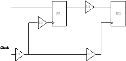
Figure 1 Schematic diagram of the setup/hold path
PT workflow
Figure 2 shows the workflow of the PT. We can see that static timing analysis is an iterative process. Until the results meet the requirements.
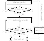
Figure 2 PT workflow
The environment in which the chip is operating is different, but the difference in environment causes the delay of the cells and lines inside the chip to be different. In order to make the chip work in most environments, three analysis modes are provided in the PT: single, bc_wc, on_chip_variation. We usually use the bc_wc mode, which divides the environment process, temperature, and voltage into the following three cases:
1, best case: process: 1; ideal temperature minus 40 degrees Celsius; voltage 1.32V (the rated voltage of this chip is 1.2V)
2, typical case: process: 1; room temperature environment 25 degrees Celsius; voltage 1.2V
3, worst case: process: 1; 125 degrees Celsius; voltage 1.08V
In order to test whether the chip has physical defects such as the production and packaging of the entire production process, the function is incorrect. DFT (Design for Test) circuits have been added to the design of VLSIs. When the chip is operating in test mode, the structure of the clock tree is completely different from the functional mode. We must also do static timing analysis in the above three cases in the test mode.
3. Relationship between static timing analysis and gate level simulation
Static timing analysis also has its own weaknesses, which cannot verify the correctness of circuit functions. It is worth noting that the static timing analysis can only effectively verify the correctness of the synchronization timing. Most of the designs may include the timing verification of the asynchronous circuit. The gate-level simulation must be used to ensure the correctness of the timing.
According to the above introduction to static timing analysis, we should also simulate the case of best case, typical case, and worst case in functional mode and test mode, but the focus is different. In the functional mode, most of the circuits we only need to verify the worst case and the best case can be considered correct, but in the design of our chip, there have been cases where the worst case and the best case pass and the typical case fails. This is because there are too many register stages in some circuits, and the clock skew affects the circuit. Although this situation is rare even in the design of more than a million gates, in order to improve the chip success rate, for the critical path, the key modules need to simulate the situation in 3. The test mode generally works in a room temperature environment, and its simulation only needs to be concerned with the typical case.
The static timing analysis tool cannot verify the circuit of the asynchronous clock. However, there may be asynchronous clock circuits in the chip. For example, in our TDS-CDMA digital baseband processing chip, there are more than twenty asynchronous clock domains. In the PT, the path of all asynchronous clock domains must be set to false_path (indicating that the path is not of concern). Since the RTL-level functional simulation cannot also detect signal errors between asynchronous clock domains, we need to pay special attention to the verification of signals between asynchronous clock domains during gate-level simulation.
We may also encounter a door-level simulation failure, but there is no error in the PT. After trial and error analysis, there may be several situations in which their results are inconsistent:
1. VCS does not support negative input and output path delays, but PT is supported. When VCS encounters a negative input and output path delay, it automatically considers it to be zero. This leads to errors.
2. The SDF file generated by the new version of the PT has information about the edge of the signal. If we do not include this edge information with an older version of the library or memory model, the PT will consider it a longer path. While VCS is still calculated with standard delays, the results are inconsistent. It can be seen that a complete set of EDA tools is complex, and the nuances between different versions may also lead to the failure of our verification.
3. The most common reason is that the `timescale is different. If the design and the `timescale set in the SDF file are different, the inverse value in the SDF file may be discarded. This leads to a mismatch between static timing analysis and dynamic simulation. Therefore, it is very important to ensure that the 'timescale' in the RTL code, library file, memory model, and SDF file is consistent.
Gate level simulation is the last verification before chip streaming. Although it can reflect the real situation of the chip work well, the resource is occupied seriously and the time is long. Only by comprehensively utilizing the advantages of dynamic verification and static verification can the design of a chip be completed efficiently and accurately.
4. Application in TDS-CDMA digital baseband processing chip
The object of our experiment is the TDS-CDMA digital baseband processing chip, which is a very large-scale integrated circuit with a size of more than 10 million gates and 130nm process, including hard cores such as ARM and DSP. It is unrealistic to do a full-featured test at the gate level that requires a lot of human and material resources. We use static timing analysis plus gate-level simulation in the actual chip design.
In the design process of the chip, we do static timing analysis in several stages.
1) Make a STA first after synthesis. The main check at this time:
1. There is no problem with the timing of the circuit design. If there is too much combinational logic between the two registers, the circuit cannot run at the required clock frequency.
2. Due to the algorithmic limitations of the integrated tools (Design Complier in the design), the netlists are different each time. It needs to be synthesized repeatedly until the timing of the netlist reaches our expectations. Use this version of the netlist to continue to do it.
Since there is no specific place and route information, the timing analysis at this time is established on the wire load model. The online load model is a more pessimistic model, so there may be some Violation that is not very serious. At this stage we don't need to care about these, they can be solved during place and route.
2) After pre-layout:
At this time, the approximate positional relationship of the components has been determined. Static timing analysis can be used to solve unreasonable places in the layout for modification.
3) After the layout and layout is completed:
After place and route, you can extract the exact device and network delay from the layout to get the SPEF (Standard Parasitic Exchange Format) file, and then perform the timing analysis in the Prime Time SI. Then you can get the accurate timing analysis results based on the layout.
In the process of place and route, it is necessary to use STA to analyze the result of layout and routing. Our chips use a 0.13 micron process library from SMIC. They offer both a standard component library and an HVT component library. The HVT component is characterized by low leakage, but the delay is relatively large. Therefore, at the beginning we used HVT components, and after doing the STA, we found that some paths could not meet the timing requirements. We replace these HVT components with some standard components and repeat the comparison until all the paths meet the timing requirements. In this way, both low power consumption and timing requirements are met to the greatest extent.
After the timing analysis is completed, the SDF (standard delay format) file is generated by the PT SI and the target level is simulated in the netlist.
The SDF file at this time includes not only the unit delay and the line delay, but also the layout information, crosstalk information, and the like. Gate-level simulation can get the most realistic and closest results to the actual situation.
5. Conclusion
Static timing analysis is fast and consumes less memory. It can perform comprehensive timing function check on the chip design and optimize the design by using the results of timing analysis. It is quickly used to verify the design of digital integrated circuits. in. However, gate-level simulation is still a place in ASIC design due to its irreplaceable position. Combined with the experience in the design of TDS-CDMA digital baseband processing chip, we can draw the conclusion that static timing analysis and gate-level timing simulation are to analyze the circuit from different focuses to ensure the timing of the circuit is correct, they are complementary. . Now, the experimental TDS-CDMA digital baseband processing chip has been successfully streamed.
The author of this paper is innovative: in practice, a new method combining STA and gate-level simulation is found. Maximize the time for chip verification on the basis of guaranteeing the success rate of the stream.
Pcba,Multilayer Pcb,Double-Sided Pcb,Single-Sided Pcb
PCB Assembly Co., Lt d , http://www.nbmultilayerpcb.com