Abstract: This article compares the differences between DS26303 and LXT384, especially how to use DS26303 in existing LXT384 applications, and elaborate on the differences in features, considerations in register and hardware design
Overview This article compares the differences between DS26303 and LXT384, especially how to use DS26303 in existing LXT384 applications. The DS26303 is an 8-channel E1 / T1 / J1 short-range line interface unit (LIU) powered by a single 3.3V. It can support the function of LXT384 without changing the software, and it can provide additional features through the extended register set. No need to change the PCB, DS26303 can be used in the existing LXT384 application, only need to change the value of peripheral components according to the application.
The difference in characteristics is divided into three different parts: Table 1 shows some features that DS26303 has but LXT384 does not; Table 2 shows some features that LXT384 has but DS26303 does not. Table 3 shows the common features of DS26303 and LXT384 but different features implemented on the two devices.
Table 6 to Table 10 are the differences between the DS26303 and LXT384 registers and the additional functions provided by the DS26303 extended register set. Figure 1 and Table 11 show the subtle changes to the device values ​​when using the DS26303 in existing LXT384 applications.
Table 1. Features of DS26303 different from LXT384
Table 2. Characteristics of LXT384 different from DS26303
Table 3. Differences in features shared by DS26303 and LXT384
Table 4. DS26303 MCLK selection range
Table 5. DS26303 clock A selection range
Register considerations DS26303 includes four main register groups. Main register set (DS26303 and LXT384) Secondary register set (DS26303 unique) Independent LIU register set (DS26303 unique) BERT register set (DS26303 unique) Except for one, the main register of DS26303 is the same as the register in LXT384 . The reserved register with the address of 1Fh in LXT384 becomes the address pointer (ADDP) of its additional register bank in DS26303. If DS26303 replaces the existing LXT384, there is no need to modify the application software. Table 6 is a list of DS26303 and LXT384 main register groups.
Table 6. Main register set of DS26303 and LXT384
In order to take advantage of the additional features and flexibility of DS26303, programs must be added to the source code of all LXT384 applications. The address of the ADDP register in DS26303 is 1F (hexadecimal). This address is reserved in LXT384. ADDP is used as a pointer to access different register sets. Table 7 is the DS26303 register set list and the ADDP values ​​required when accessing different register sets.
Table 7. DS26303 address pointer selection
Table 8 is a list of registers included in the secondary register set, Table 9 is a list of registers included in the independent LIU register set, and Table 10 is a list of registers included in the BERT register set.
Table 8. DS26303 secondary register set
Table 9. Independent LIU register set of DS26303
Table 10. BERT register set of DS26303
Hardware considerations The DS26303 can be used to replace the LXT384 in existing applications without changing the PCB. What needs to be done is to change the external device value according to the target application. Figure 1 shows the recommended network termination circuit for the DS26303, and Table 11 shows the device values ​​required when the DS26303 is properly terminated.
Transmitter LXT384 requires that the transmitter-side resistors be connected in series to the TTIP and TRING outputs. It is recommended that these resistors should be 0Ω (T1 3.3V mode), 11Ω (E1 75Ω coaxial) or 11Ω (E1 120Ω twisted pair). DS26303 does not require resistance, so the resistance in all modes should be 0Ω. When pulse shaping is disabled, the LXT384 requires a DC isolation capacitor. DS26303 does not require a DC isolation capacitor, so if there is a capacitor in the PCB circuit of the existing LXT384 application, it can be replaced with a 0Ω resistor.
The receiver is on the receiving side. LXT384 requires a termination impedance of 12.4Ω (T1 3.3V mode), 9.31Ω (E1 75Ω coaxial) or 15Ω (E1 120Ω twisted pair). When using the external impedance mode, the DS26303 requires a 15Ω termination resistor in all cases; when using the DS26303 software to select the impedance matching mode, no resistance is required. LXT384 requires a 1kΩ resistor in series with the RTIP and RRING pins. If the DS26303 uses software to select the termination / impedance matching mode, these 1kΩ resistors can be replaced with 0Ω resistors.
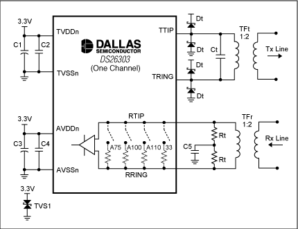
Figure 1. LIU front-end circuit diagram
Table 11. LIU front-end values
Overview This article compares the differences between DS26303 and LXT384, especially how to use DS26303 in existing LXT384 applications. The DS26303 is an 8-channel E1 / T1 / J1 short-range line interface unit (LIU) powered by a single 3.3V. It can support the function of LXT384 without changing the software, and it can provide additional features through the extended register set. No need to change the PCB, DS26303 can be used in the existing LXT384 application, only need to change the value of peripheral components according to the application.
The difference in characteristics is divided into three different parts: Table 1 shows some features that DS26303 has but LXT384 does not; Table 2 shows some features that LXT384 has but DS26303 does not. Table 3 shows the common features of DS26303 and LXT384 but different features implemented on the two devices.
Table 6 to Table 10 are the differences between the DS26303 and LXT384 registers and the additional functions provided by the DS26303 extended register set. Figure 1 and Table 11 show the subtle changes to the device values ​​when using the DS26303 in existing LXT384 applications.
Table 1. Features of DS26303 different from LXT384
| DS26303 | LXT384 |
| Programmable opTIons to clear interrupt status on write or read. Clear on read is default. | Not supported. |
| Individual channel control for jitter attenuator: Enable / disable FIFO depth FIFO limit trip | All channels have global control. |
| Internal software-selectable transmit and receive side terminaTIon for 100Ω T1 twisted-pair, 110Ω J1 twisted-pair, 120Ω E1 twisted–pair, and 75Ω E1 coaxial applicaTIons. | Not supported. |
| In HPS mode, the transmitter output and the internal impedance of the receiver can be turned off with only the OE pin. | Requires that both receivers use the same front-end terminaTIon. |
| Built-in BERT tester for diagnostics. | Not supported. |
| Individual channel control for: Short-circuit protection AIS enable on LOS RCLK inversion TCLK inversion | All channels have global control. |
| Individual channel-line violation detection. | Not supported. |
| Flexible MCLK See Table 4 for available input frequencies. | Not supported. |
| Programmable TECLK output pin (1.544MHz or 2.048MHz) | Not supported. |
| Programmable CLKA output pin See Table 5 for available output frequencies. | Not supported. |
| Flexible interrupt pin | Not supported. |
Table 2. Characteristics of LXT384 different from DS26303
| DS26303 | LXT384 |
| Uses single optimal value. | Capability to select the jitter attenuator bandwidth. |
| — | Analog JTAG |
| MLCK Pin Functionality The DS26303 and LXT384 both require MCLK to for data with clock recovery as well as AIS detection. The MCLK pin of the LXT384 provides additional functionality not present in the DS26303. LXT384 MCLK held high. The LXT384 operates as a simple data receiver. The clock-recovery circuit is disabled and RPOS / RNEG are internally connected to an EXOR that is fed to the RCLK pin for external clock recovery. The PLL recovery circuit is disabled in this mode. LXT384 MCLK held low. RPOS / RNEG and RCLK go to a high-impedance state. | |
Table 3. Differences in features shared by DS26303 and LXT384
| DS26303 | LXT384 |
| 3.3V LIU power only, 5V not provided. | 5V LIU power. |
| Non-mux Intel® write address to WRB rising-edge setup time is 17ns. | Non-mux Intel write address to WRB rising-edge setup time is 6ns. |
| Expects non-mux Intel read address to be valid when RDB is active. | Non-mux Intel read address to RDB rising-edge setup time is 6ns. This might be an error in datasheet because data is out before this setup time. |
| Inactive RDY to tri-state delay time 12ns (max). | Inactive RDY to tri-state delay time 3ns (max). |
| Clears the interrupt pin when reading or writing the interrupt status. | Clears interrupt pin when reading the status register. |
| Jitter attenuator FIFO depths of 32 bits or 128 bits. | Jitter attenuator FIFO depths of 32 bits or 64 bits. |
| Individual channel control for jitter attenuator: Enable / disable FIFO depth FIFO limit trip | All channels have global control. |
Table 4. DS26303 MCLK selection range
| PLLE | MPS1, MPS0 | MCLK MHz (± 50ppm) | FREQS | T1 or E1 Mode |
| 0 | xx | 1.544 | x | T1 |
| 0 | xx | 2.048 | x | E1 |
| 1 | 00 | 1.544 | 1 | T1 / J1 or E1 |
| 1 | 01 | 3.088 | 1 | T1 / J1 or E1 |
| 1 | 10 | 6.176 | 1 | T1 / J1 or E1 |
| 1 | 11 | 12.352 | 1 | T1 / J1 or E1 |
| 1 | 00 | 2.048 | 0 | T1 / J1 or E1 |
| 1 | 01 | 4.096 | 0 | T1 / J1 or E1 |
| 1 | 10 | 8.192 | 0 | T1 / J1 or E1 |
| 1 | 11 | 16.384 | 0 | T1 / J1 or E1 |
Table 5. DS26303 clock A selection range
| CLKA3 to CLKA0 | MCLK (Hz) |
| 0000 | 2.048M |
| 0001 | 4.096M |
| 0010 | 8.192M |
| 0011 | 16.384M |
| 0100 | 1.544M |
| 0101 | 3.088M |
| 0110 | 6.176M |
| 0111 | 12.352M |
| 1000 | 1.536M |
| 1001 | 3.072M |
| 1010 | 6.144M |
| 1011 | 12.288M |
| 1100 | 32k |
| 1101 | 64k |
| 1110 | 128k |
| 1111 | 256k |
Register considerations DS26303 includes four main register groups. Main register set (DS26303 and LXT384) Secondary register set (DS26303 unique) Independent LIU register set (DS26303 unique) BERT register set (DS26303 unique) Except for one, the main register of DS26303 is the same as the register in LXT384 . The reserved register with the address of 1Fh in LXT384 becomes the address pointer (ADDP) of its additional register bank in DS26303. If DS26303 replaces the existing LXT384, there is no need to modify the application software. Table 6 is a list of DS26303 and LXT384 main register groups.
Table 6. Main register set of DS26303 and LXT384
| Address (Hex) | DS26303 | LXT384 |
| 00–15 | Primary Registers | Registers |
| 16–1E | Reserved | Reserved |
| 1F | ADDP (Address pointer for additional register banks). This register must be set to point to the desired register bank. 00h) Primary Bank AAh) Secondary Bank 01h) Individual LIU Bank 02h) BERT Bank | Reserved |
In order to take advantage of the additional features and flexibility of DS26303, programs must be added to the source code of all LXT384 applications. The address of the ADDP register in DS26303 is 1F (hexadecimal). This address is reserved in LXT384. ADDP is used as a pointer to access different register sets. Table 7 is the DS26303 register set list and the ADDP values ​​required when accessing different register sets.
Table 7. DS26303 address pointer selection
| ADDP7 to ADDP0 (Hex) | Bank Name |
| 00 | Primary Bank |
| AA | Secondary Bank |
| 01 | Individual LIU Bank |
| 02 | BERT Bank |
Table 8 is a list of registers included in the secondary register set, Table 9 is a list of registers included in the independent LIU register set, and Table 10 is a list of registers included in the BERT register set.
Table 8. DS26303 secondary register set
| Address (Hex) | Register Name |
| 00 | Single-Rail Mode Select |
| 01 | Line-Code Selection |
| 02 | Not used |
| 03 | Receiver Power-Down Enable |
| 04 | Transmitter Power-Down Enable |
| 05 | Excessive Zero-Detect Enable |
| 06 | Code-Violation-Detect Enable Bar |
| 07–1E | Not used |
| 1F | Set to AAh for access to Secondary Register Bank |
Table 9. Independent LIU register set of DS26303
| Address (Hex) | Register Name |
| 00 | Individual JA Enable |
| 01 | Individual JA Position Select |
| 02 | Individual JA FIFO Depth Select |
| 03 | Individual JA FIFO Limit Trip |
| 04 | Individual Short-Circuit-Protection Disable |
| 05 | Individual AIS Select |
| 06 | Master Clock Select |
| 07 | Global-Management Register |
| 08–0F | Reserved |
| 10 | Bit-Error-Rate Tester Control Register |
| 12 | Line-Violation Detect Status |
| 13 | Receive Clock Invert |
| 14 | Transmit Clock Invert |
| 15 | Clock-Control Register |
| 16 | RCLK Disable Upon LOS Register |
| 1E | Global-Interrupt Status Control |
| 1F | Set to 01h for access to Individual LIU Register Bank |
Table 10. BERT register set of DS26303
| Address (Hex) | Register Name |
| 00 | BERT Control Register |
| 01 | Reserved |
| 02 | BERT Pattern Configuration 1 |
| 03 | BERT Pattern Configuration 2 |
| 04 | BERT Seed / Pattern 1 |
| 05 | BERT Seed / Pattern 2 |
| 06 | BERT Seed / Pattern 3 |
| 07 | BERT Seed / Pattern 4 |
| 08 | Transmit-Error Insertion Control |
| 09–0A | Reserved |
| 0C | BERT Status Register |
| 0D | Reserved |
| 0E | BERT Status Register Latched |
| 10 | BERT Status Register Interrupt Enable |
| 11–13 | Reserved |
| 14 | Receive Bit-Error Count Register 1 |
| 15 | Receive Bit-Error Count Register 2 |
| 16 | Receive Bit-Error Count Register 3 |
| 17 | Receive Bit-Error Count Register 4 |
| 18 | Receive Bit Count Register 1 |
| 19 | Receive Bit Count Register 2 |
| 1A | Receive Bit Count Register 3 |
| 1B | Receive Bit Count Register 4 |
| 1C–1E | Reserved |
| 1F | Set to 02h for access to BERT Register Bank |
Hardware considerations The DS26303 can be used to replace the LXT384 in existing applications without changing the PCB. What needs to be done is to change the external device value according to the target application. Figure 1 shows the recommended network termination circuit for the DS26303, and Table 11 shows the device values ​​required when the DS26303 is properly terminated.
Transmitter LXT384 requires that the transmitter-side resistors be connected in series to the TTIP and TRING outputs. It is recommended that these resistors should be 0Ω (T1 3.3V mode), 11Ω (E1 75Ω coaxial) or 11Ω (E1 120Ω twisted pair). DS26303 does not require resistance, so the resistance in all modes should be 0Ω. When pulse shaping is disabled, the LXT384 requires a DC isolation capacitor. DS26303 does not require a DC isolation capacitor, so if there is a capacitor in the PCB circuit of the existing LXT384 application, it can be replaced with a 0Ω resistor.
The receiver is on the receiving side. LXT384 requires a termination impedance of 12.4Ω (T1 3.3V mode), 9.31Ω (E1 75Ω coaxial) or 15Ω (E1 120Ω twisted pair). When using the external impedance mode, the DS26303 requires a 15Ω termination resistor in all cases; when using the DS26303 software to select the impedance matching mode, no resistance is required. LXT384 requires a 1kΩ resistor in series with the RTIP and RRING pins. If the DS26303 uses software to select the termination / impedance matching mode, these 1kΩ resistors can be replaced with 0Ω resistors.
Figure 1. LIU front-end circuit diagram
Table 11. LIU front-end values
| Mode | Component | 75 | 120 | 100 |
| Tx Capacitance | Ct | 560pF (typ). Adjust for board parasitics for optimal return loss. | ||
| Tx Protection | Dt | International Rectifier: 11DQ04 or 10BQ060 Motorola: MBR0540T1 | ||
| Rx Transformer 1: 2 | TFr | Pulse: T1124 (0 ° C to + 70 ° C) | ||
| Tx Transformer 1: 2 | TFt | Pulse: T1114 (-40 ° C to + 85 ° C) | ||
| Tx Decoupling (ATVDD) | C1 | Common decoupling for all eight channels is 68µF. | ||
| Tx Decoupling (ATVDD) | C2 | Recommended decoupling per channel is 0.1µF. | ||
| Rx Decoupling (AVDDn) | C3 | Common decoupling for all eight channels is 68µF. | ||
| Rx Decoupling (AVDDn) | C4 | Common decoupling for all eight channels is 0.1µF. | ||
| Rx Termination | C5 | When in external impedance mode, Rx capacitance for all eight channels is 0.1µF. Do not populate if using internal impedance mode. | ||
| Rx Termination | Rt | When in external impedance mode, the two resistors for all modes is 15.0Ω ± 1%. Do not populate if using internal impedance mode. | ||
| Voltage Protection | TVS1 | SGS-Thomson: SMLVT 3V3 (3.3V transient suppressor) | ||
China leading manufacturers and suppliers of Brushless Dc Servo Motor,Brushless Dc Servo Motors, and we are specialize in Dc Servo Motor In Robotics,Servomotor For Vehicle Robot, etc.
Motor Voltage: 12V 24V 48V
Motor Power: 100w 200w 400w 500w 750w 800w 1000w 1200w 1500w 2000w 3000w
Motor speed: 1500rpm 3000rpm
Encoder: 2500ppr, optical, if you need other type encoder, please advise.
The motor also be named pmsm motor, permanent-magnet synchronous motor, sinusoid wave, be widely used in robot vehicle.
Brushless Dc Servo Motor
Brushless Dc Servo Motor,Brushless Dc Servo Motors,Dc Servo Motor In Robotics,Servomotor For Vehicle Robot
Jinan Keya Electron Science And Technology Co., Ltd. , https://www.keyaservo.com