Wireless transmission of data has been developed for some time. Today, consumers are eager to have wireless charging capabilities, and technology enablers are actively responding to this demand. In this article, Infineon will review and compare current state-of-the-art methods and technologies and illustrate the benefits of integrated wireless charging solutions.
backgroundEvery electronic device requires power, but there is very little wireless power, and most of it is powered from a wall outlet through an adapter. The term "wireless" is now synonymous with data transmission. However, the radio magnetic field can also transfer power to the device, providing greater convenience to the user. Since no cables are required, compatibility issues are reduced and the safety and reliability of the equipment is improved.
By removing all the interfaces, the device is easier to seal, which helps the device to be rugged and to benefit the consumer, as one in five smartphones accidentally fell into the liquid. The biggest advantage of wireless charging is getting rid of the bulky charging adapter.
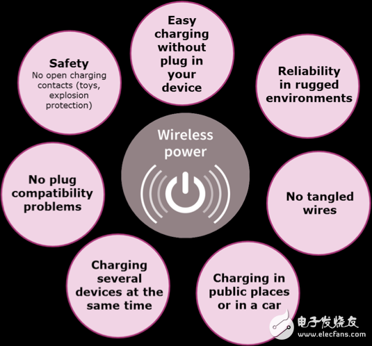
Figure 1: Wireless charging brings many benefits to users and device manufacturers
As the industry moves to universal charging solutions, there may be more and more public charging stations in airports, hotels, event venues, fast food chains, coffee shops and other places.
Designers face challengesMost chargers are switch-mode power supplies that need to master electromagnetism - many engineers think this is a "magic." Wireless charging is also performed in a similar manner - except that the transformer is separated from the charger and the device to be charged. Therefore, the term has also changed - the primary side becomes the "transmitter" and the secondary side becomes the "receiver".
In wireless charging, the coil and its coupling have a greater impact on overall performance than the SMPS. Since the wireless windings are independent, their coupling is looser than the SMPS. However, transmitters and receivers can be designed with good coupling coefficients to allow wireless charging to transfer power with unexpected efficiency.
In addition to magnetism, issues such as efficiency, mechanical packaging, electromagnetic interference (EMI), thermal management, and metallic foreign objects (such as coins and keys) present more challenges for designers.
Wireless topology and technologyWireless charging solutions typically have three key components: adapter/charger, transmitter, and receiver, as shown below.
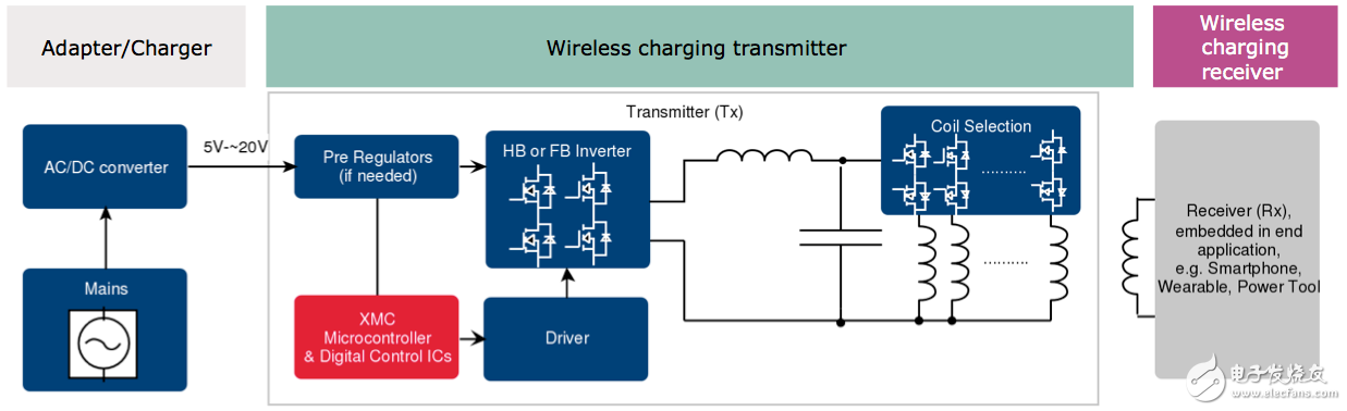
Figure 2: A typical wireless charging system consists of three main components
The adapter converts the mains and transmits a 5-20 VDC regulated power supply to the primary/transmitter. Adapters are usually separate devices that are connected to the transmitter by wires, and they can also be integrated into one unit.
The transmitter consists of a MOSFET-based half-bridge or full-bridge inverter that converts direct current into alternating current and produces an alternating magnetic field. The inverter is controlled by a microcontroller and associated MOSFET drivers to provide the flexibility and functionality required for wireless inductive charging.
Class D and Class E are two popular topologies for resonant applications. Although very similar in many respects, the advantages of the two methods are slightly different, making the two methods suitable for different applications.
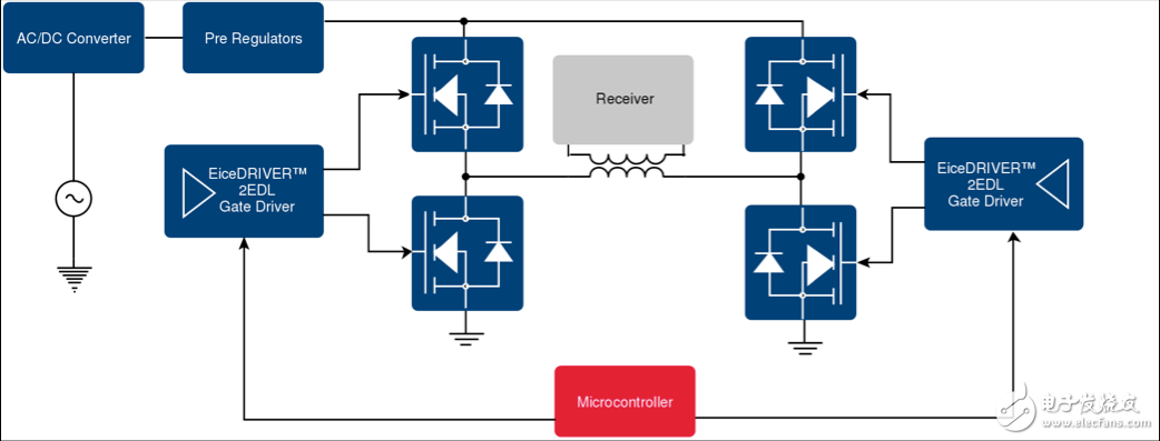
Figure 3: Class D topology for resonant applications
As shown above, Class D wireless charging is achieved through a full bridge topology. A half bridge topology can also be used. Class D provides a nearly flat efficiency curve over a wide load range and is therefore suitable for use in general purpose wireless charging stations, such as in public places where various devices can be recharged. This method is suitable for a wide range of power levels.
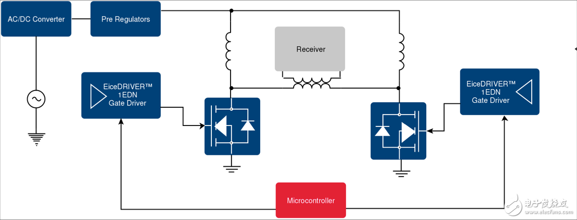
Figure 4: Class E topology for resonant applications
The E class topology is shown in the figure above. This can be used in single-ended or differential mode (as shown). Unlike Class D topologies, Class E topologies are optimized for specific parameter sets and will exhibit greater efficiency at a particular point. However, class E topology efficiency drops rapidly outside of this point. Therefore, Class E topologies are the best choice for higher power levels and charging for near target power or fully uncharged devices. The cost of class E BOM is slightly lower than that of class D, but the difference is not big.
Infineon offers a complete package solution for wireless charging transmitters and switch mode power supplies for converting mains AC to inverter input DC.
The choice of a wide range of wireless charging products gives design engineers the confidence to use components and subsystems that are guaranteed to be compatible.
The microcontroller, which is the core of the transmitter design, is responsible for system control/intelligence. Infineon's XMCTM microcontroller family offers designers a wide range of options, and the XMC1100, 1402 and XMC4108 are ideal for wireless charging Class D and Class E topologies.
The EiceDRIVERTM gate driver converts the microcontroller signal to drive the MOSFET directly. The new 2EDL71 is best suited for Class D design, while the proven 1EDN is the first choice for Class E applications.
Infineon offers a wide range of MOSFETs. Specific specification differences include package size and important parameters (such as RDS(ON) and Qg), where Infineon has an industry-leading figure of merit (FoM). A wide range of voltage levels from 30 V to 250 V are available, giving designers the flexibility to use the same circuitry to design wireless chargers of multiple power levels. Infineon's market-leading OpTIMOSTM MOSFETs are used in Class D or Class E inverters (and synchronous rectification), while the CE and P7 versions of CoolMOSTM devices provide switching for ACDC adapters.
Infineon also offers a range of flyback controllers for power adapters, as well as CoolSETTM with integrated controller and power unit.
To support component solutions, Infineon's newly developed Class D power amplifier transmitter test board allows designers to quickly begin designing and developing efficient and compact solutions.
The test board allows designers to evaluate the functionality and performance of Infineon MOSFETs in Class D power amplifiers. The test board consists of two half-bridges consisting of an 80V 2x2 Infineon MOSFET (IRL80HS120) and associated drivers, allowing the user to operate between a single-ended configuration (only one half-bridge operation) and a differential configuration (both half-bridges are active) Switch.
The embedded oscillator ensures an accurate 6.78 MHz operating frequency and provides a pin to set the switching frequency with an external waveform generator (via the BNC connector).
Includes all the necessary components to design a zero voltage switching (ZVS) power solution to achieve maximum efficiency. The on-board linear regulator provides a stable supply voltage for the board logic.
The second BNC connector can be connected to an external transmit coil for radio energy transmission. If you can use a wireless charging receiver, you can create a complete wireless charging design.
to sum upWireless charging brings the same benefits as wireless data transmission. With the integration of standards and methods, increased interoperability between all chargers and portable devices will bring more convenience to users. Continuous integration and innovation will bring true “wireless charging†convenience and increased power levels, enabling more types of devices to be wirelessly charged.
As a leading supplier, Infineon has a wide range of products including all key components of AC adapters and transmitters. Each component features a high level of performance, including low switching/conduction losses, a low parasitic package, and a high figure of merit, FoM, enabling designers to build wireless charging solutions with proven silicon MOSFET technology. Infineon's extensive experience in power semiconductors and microcontrollers has made it a technology and quality leader.
Test boards that accelerate product evaluation and development support a broad portfolio of products that comprehensively cover wireless charging designs. Infineon offers advanced products and valuable ecosystem support to current and future wireless charging solution designers.
Author:
Stephan Schächer, Head of Technology and Systems Marketing, Infineon Technologies DCDC
Milko Paolucci, Senior Application Engineer, Infineon Technologies
ZGAR PCC KIT
ZGAR electronic cigarette uses high-tech R&D, food grade disposable pod device and high-quality raw material. All package designs are Original IP. Our designer team is from Hong Kong. We have very high requirements for product quality, flavors taste and packaging design. The E-liquid is imported, materials are food grade, and assembly plant is medical-grade dust-free workshops.
From production to packaging, the whole system of tracking, efficient and orderly process, achieving daily efficient output. We pay attention to the details of each process control. The first class dust-free production workshop has passed the GMP food and drug production standard certification, ensuring quality and safety. We choose the products with a traceability system, which can not only effectively track and trace all kinds of data, but also ensure good product quality.
We offer best price, high quality Vape Device, E-Cigarette Vape Pen, Disposable Device Vape,Vape Pen Atomizer, Electronic cigarette to all over the world.
Much Better Vaping Experience!


E-Cigarette Vape Pen,Disposable Device Vape,PCC SET, Vape Pen Atomizer,Latest Disposable E-Cigarette OEM vape pen,OEM electronic cigarette
ZGAR INTERNATIONAL TRADING CO., LTD. , https://www.zgarpods.com