Automotive electronic single chip solution based on mixed signal technology
As the electronic components of automotive components continue to increase, automotive engineers are actively seeking advanced control and interface technology solutions in vehicle systems. At present, the space and energy used to embed these functional units in automotive systems is very limited, and automotive engineers are using a new high-voltage mixed-signal technology to integrate complex, currently incompatible component functions into a single chip. Now, I3T high voltage technology compatible with 42V vehicle voltage has been able to integrate complex digital circuits (such as sensors), embedded microprocessors, and power circuits (such as excitation or switch drivers).
LIN bus system Due to its relatively low cost, LIN bus is widely used in automotive distributed control systems, such as stepper motor and DC power supply for controlling electric windows, adjusting mirrors and headlights. , or manage information about the temperature or seat position collected by the sensor. The transmission byte of the LIN bus is up to 20kbps. Based on the structure of a single master node, multiple slave nodes, typically, the slave nodes are mounted around an interface of a transceiver, a microcontroller, a sensor, or an excitation driver composed of discrete components. Recently developed a microcontroller with a LIN bus asynchronous transceiver (UART) that can be integrated with other slave modules (such as LIN bus transceivers, voltage regulators, watchdog timers). The accessories for the excitation drive and sensor interface are used together. At present, AMI Semiconductor (AMIS) uses mixed-signal technology to integrate all key node modules into a single-function, low-power, standard-compliant IP chip, which has further advanced the development of the LIN bus. The features of the program are:
Integrated RC oscillator with error ≤15%;
Dedicated IP module (such as DC or micro stepper motor driver);
Compliance with the LIN bus V1.3 protocol;
Transmission rate up to 20kbps (special structural design);
Low frequency transmission and reception;
Low current consumption in sleep/bypass mode;
Meet potential market needs.
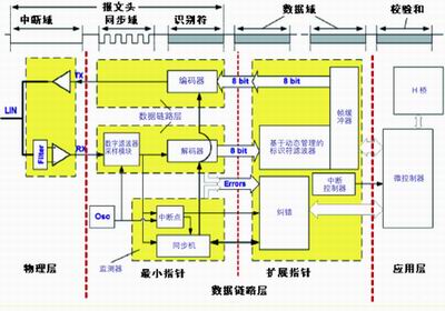
Figure 1 is a block diagram of the main components of a slave node integrated with a LIN bus. The AMIS solution provides all the major functional modules required by the application layer and the data link layer. These functional modules can be programmed in VHDL code and evaluated using the AMIS development board, which will be briefly described below.
Sampling module with digital filter The module collects the signal from the receiver and passes the resulting data stream through a digital filter to remove spurious transmissions due to attenuation of the LIN bus signal. As a result, the module improves the performance of the LIN protocol in harsh environments and minimizes problems in synchronization and data sampling.
Synchronizer The Synchronizer module extracts the required information from the sync domain to determine the exact sample rate of the encoder and decoder. The module has an internal crystal and uses a technique that minimizes the occasional rounding errors in traditional UART technology. The main advantage of the synchronous machine is that the LIN protocol can be executed with a lower clock frequency. For example, a 250KHz master clock and a 15% tolerance can be used to achieve accurate communication. In addition, the AMIS solution achieves a wide range of duty cycle variations. A typical UART can achieve a duty cycle of 33 to 66% with zero crystal error. However, the AMIS solution can achieve a duty cycle of 12 to 88% and can fully adapt to the crystal error. While providing a large tolerance to the physical layer parameters, it also improves the electromagnetic compatibility that has a large influence on the duty ratio.
Identifier filter and its dynamic management The master node issues different slave instruction identifiers during the initial and running of the system. To do this, the slave node will contain a certain number of registers. The ROM instruction number array refers to different instructions executed from the node, and contains corresponding identifiers in the RAM or EEPROM. The address register module identifies different slave nodes on the same LIN bus, while the second ROM array identifies different slave nodes for different applications and executions. The identifier filter determines the execution of the instruction according to the assigned identifier. If the identifier exists in the queue, the instruction is executed, otherwise it is not executed.
Error Correction The error identification module is at the data link layer, while error correction is performed at the application layer. Therefore, the amount of error is defined in the software by the embedded microcontroller. The error correction module in the application layer contains a status register, each of which has a corresponding error flag, and an interrupt request is generated by the flag bit to the core of the microprocessor. The error flag can be cleared by performing a read operation on the status register. Each error directly interrupts communication, resulting in a bit error to stop sending bytes. In turn, this frame information is ignored and the slave node waits for the next interrupt domain.
Frame Buffer The frame buffer is another way to minimize interrupts to the microprocessor core. It works with the identifier filter to reduce the number of interrupts to once per frame. The buffer contains 17 bytes (one identifier, eight transmit bytes, eight receive bytes).
Kernel/State Machine and Application Interface AMIS provides different cores as needed. The core and the LIN controller are connected by an interrupt signal and a special function register (SFR). The LIN controller can be regarded as a peripheral device on the SFR bus. In addition to these LIN bus features, like the same semiconductor processing technology platform, AMIS has developed a wide range of IP module libraries, including è´°(2) and SAR ADC modules, delay flip-flops with output currents up to 0.3A, and output currents up to 3A. H bridge. Of course, the use of slave nodes is only part of the overall function, and providing them with enough power to integrate them into today's cars is the next major challenge for automotive electrical engineers.
42V Power Technology Solution In an ideal automotive power solution, the power level will be converted from a traditional 12V battery voltage to a 42V power system. In the 42V system, the power level will continue to rise. For example, the maximum operating voltage for the entire life cycle of the system is set at 50V. If there is a maximum dynamic overvoltage of 8V, the supply voltage will reach 58V. Adding a 12V external drive load pump will increase the system's voltage requirements to 70V, and add an ESD protection window to achieve a system voltage of 80V. Moreover, automotive semiconductor devices must not only withstand higher voltages, but must also be robust enough to meet their demanding operating conditions, such as operating temperatures ranging from -40 ° C to +200 ° C. To date, the need to withstand higher voltages and meet demanding operating conditions is a major obstacle to the application of intelligent SoC technology in 42V automotive electronics systems.
AMI Semiconductor's I3T80 is an 80V power intelligent module integration technology based on 0.35mm CMOS technology. Meet the harsh operating conditions of the 42V automotive system. Devices developed by this technology include motor control drivers, DC-DC converters, high-precision analog circuits with bandwidth filters, and ADCs and DACs. And I3T80 can embed and integrate more than 150,000 gates, and its communication protocol modules include PLL, USB, bus protocol controller, CAN and LIN communication controller. In addition, it also provides ROM and RAM memory.
Conclusion In new automotive electronics applications, as electronic components continue to increase, automotive designers are looking for a reasonable solution. In this way, a highly integrated, highly reliable SoC solution emerges as the times require. This solution technology requirement simplifies the execution steps and reduces the cost of control and interface with different electronic systems. AMIS's high voltage, mixed-signal technology meets this need. It combines a semiconductor solution with a dedicated IP module to meet any standard interface communication bus (LIN, CAN) node application while being compatible with the 42V voltage level scheme.
Product categories of Disc Stylus Pen, We are the specialized manufacturer of Stylus Pen from China. Disc Stylus Pen no need to charge, you can use it directly, it is universal, it is compatible with all brands capacitive touch screens, such as Apple, Huawei, Samsung, Xiaomi, Microsoft, Google Chrome, ect. OEM / ODM are welcome, looking forward to our cooperation.
Disc Stylus Pen,Digital Stylus Pen,Cute Ballpoint Pen,2 In 1 Stylus Pencil
Shenzhen Ruidian Technology CO., Ltd , https://www.szwisonen.com