OLED display technology is a comprehensive technology with multi-disciplinary and multi-disciplinary technologies, covering semiconductor, organic chemistry, inorganic chemistry, thin film electronics, vacuum physics, optics, etc. The key technologies involved are TFT technology, colorization technology, and organic film formation. Technology, device packaging technology, etc., and each key technology has many different technical routes, and each technology route has its own advantages and disadvantages, which is not only the difficulty of OLED technology, but also the charm of OLED technology. It is also a hot topic that the OLED industry can't talk about, and it's unclear and very much.
Four technical routes vary
AMOLED requires higher TFT technology than LCD, and the reason for this difference is that AMOLED is a current-driven device.
TFT technology, from the name point of view, has been matured in the LCD industry for many years, and has developed to the 10th generation line, but just like the same engine, the aircraft engine is not the same as the car engine, AMOLED requirements for TFT technology than LCD High, the two are not exactly the same. The essential reason for this difference is that AMOLEDs are current-driven devices and require TFTs to operate in a linearly amplified state. LCDs are voltage-driven devices, and TFTs only need to operate in a switching state. Therefore, the most widely used a-Si TFT technology in the LCD industry has the advantages of good uniformity, simple process, mature technology and low cost. However, due to its low carrier mobility, the ability to drive OLEDs is insufficient, and The problem of threshold voltage drift is a fatal shortcoming of OLEDs with poor performance stability of devices. Therefore, it is unanimously considered by the industry to be unsuitable for AMOLEDs. LTPS TFTs have the advantages of high carrier mobility and stable threshold voltage, and have been successfully used in small and medium-sized enterprises in recent years. Dimensional LCD; IGZO is one of MOTFT (Metal Oxide TFT), TFT characteristics are between a-Si and LTPS, LGD's 55-inch AMOLED is IGZO; OTFT (Organic TFT) is used for flexible display Advantageous TFT technology uses organic materials (such as pentacene) instead of silicon as a semiconductor material, but the technology is still in the basic research stage.
OLED colorization technology mainly includes RGB-SBS (RGB-Side-Side), W+CF (color filter method, also called "white light + color filter film" method) and CCM (color conversion method) , color conversion method) three. Among them, RGB-SBS adopts red, green and blue three-color organic light-emitting materials and is placed on the substrate, and RGB pixels emit light independently. This method is the most mature and mass-produced technology, and has high luminous efficiency, but due to three-color luminous efficiency. And the life is different and there may be problems with color distortion; W+CF technology follows the principle of full color LCD, using color filters to filter out the three primary colors, but using white light OLED illumination, this method can improve RGB- Two problems with SBS, but due to the attenuation of light by color filters, it is a prerequisite to develop high-efficiency and stable white OLEDs; CCM technology will generate blue and OLEDs by changing color media (CCMs) to form red and green. The pixels of light form a three-primary color together with the blue-light pixels. The advantage of this method is the same as that of the color filter method, but the efficiency is very low and the color purity is also poor. There is no mass production case yet.
Organic film-forming technology is a unique core technology of OLED. Since the thickness of the organic film in OLED devices is very thin, it is generally equivalent to about one percent of the hair diameter, and the thickness of the electron injecting layer is even less than 20 angstroms (1 angstrom = 0.1 nm). ), and the sub-pixel film is extremely fine, and the length and width are about several tens of micrometers. Therefore, it is one of the common technical problems faced by the industry to make a multi-layered fine organic film which is so thin and has no pinholes.
Organic film forming technology can be divided into three types: vacuum evaporation, laser transfer and wet preparation. Vacuum evaporation is mainly based on FMM (Fine-Metal-MASK, fine metal mask) technology. The technique of depositing organic materials in a crucible to evaporate and deposit a film on a glass substrate covered with a mask (MASK) is the most mature and currently mass-produced small-sized AMOLED products. Organic film-forming technology, but FMM technology has high requirements for alignment accuracy of MASK and glass substrate, MASK is easy to deform due to gravity and thermal expansion, and low material utilization rate; laser transfer technology is to solve the shortcomings of FMM technology. Developed, but there are still major problems such as thermal damage, process stability and productivity, which have not been used in mass production. Among them, LITI (Laser Induced Thermal Image) technology is owned by SMD and LIPS (Laser Induced Pattern wise Sublima TIon) technology is Sony owns, RIST (RadiaTIon-induced sublimaTIon transfer) technology is owned by Kodak. These technologies are very similar in principle and are all pre-existing. The material is deposited on a film called a donor by vacuum evaporation, spin coating or screen coating, and then the donor film is covered on a glass substrate (referred to as a receptor) and supplied by a laser beam. The imaging template of the body is irradiated, and as a result, the organic material on the donor portion irradiated with the laser is transferred onto the glass substrate, and finally the used donor is peeled off, so that a high-resolution organic material is obtained on the glass substrate. stripe. The three differ in the donor material used and whether the donor is in intimate contact with the receptor. Wet preparation technology is the most attractive organic film-forming technology, which has the advantages of large-area film formation, high material utilization rate, low production cost and high production efficiency. Especially R2R (volume-to-roll printing) technology is the future production flexibility. The most ideal technology for OLED, but including nozzle printing (Nozzle Printing) and inkjet printing (InkJet Printing) technology, the current wet preparation technology in the ink materials, printing equipment and process control, etc. have to be improved, the technology is still immature .
Device packaging technology is another key technology for OLEDs that is different from other display technologies. Due to the presence of water vapor and oxygen in organic materials, irreversible photooxidation reactions occur. Water and oxygen also have a strong erosive effect on electrode materials such as aluminum or magnesium silver. Therefore, OLED device packages have water and oxygen permeability. Very high demand. The traditional packaging technology for OLED devices is the “UV+glass cover†method, which first attaches a desiccant for absorbing moisture to the glass cover, then applies UV adhesive to the periphery of each display, and finally covers the glass. The glass substrate is opposite to the glass substrate after depositing the organic film, and the UV curing UV glue is used. Although the technology has the advantages of mature technology and low equipment cost, it is also easy to penetrate water, is not suitable for the top light emitting device, and is flexible display device. Disadvantages such as large-size devices; in order to apply to top-emitting AMOLEDs and improve package hermeticity, while making OLED devices thinner, Thin Film Encapsulation (TFE) and laser-sintered glass powder packaging technology (Frit) have been developed in recent years. And the new packaging technology of "Dam-Filler".
Large size, high performance is the direction
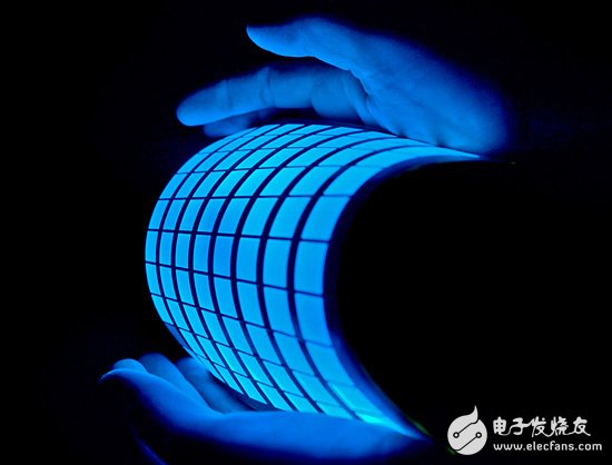
The special display product is the unique charm of OLED, and also the characteristics of the third generation display technology, bringing people's life into the magical science fiction world.
Specifically, OLED products will be developed in three major directions: first, popular display products, second, special display products, and third, lighting products. Popular display products, which are common types of displays in our daily life, such as mobile phones, tablets, computer monitors, traditional displays used in televisions, and relatively flexible displays, can also be called "rigid display." Special display products are the unique charm of OLED and the characteristics of the third generation display technology. They bring people's daily life into the magical science fiction world. There are three development directions: one is flexible display, which is as thin as paper and can be folded and folded. OLED can only display curved surface at present; the second is transparent display and double-sided display. The transparent display can observe the external environment through the screen while viewing the image displayed on the screen. The double-sided display can simultaneously be on the screen. The two sides display different images; the third is the use of OLED anti-shock, anti-vibration solid device features and operating temperature range of -40 ~ 85 ° C, developed for aerospace, aerospace, military display products. Lighting products are another major application area of ​​OLED. Due to the characteristics of surface light source, high efficiency, environmental protection and safety, especially in combination with the characteristics of flexible panels, the prospect of OLED lighting will outperform LED lighting, but OLED lighting products still need to be solved. Three issues of efficiency, long life and low cost.
In short, from the various shortcomings of OLED key technologies, we can see that the technology development trend of OLED is to solve the technical problems faced by the current industrialization and to break through the technical bottlenecks that are compatible with product development. The following aspects: First, improve the production process, improve the process yield, reduce costs; Second, break through the existing bottlenecks of low-temperature polysilicon, metal oxide and other TFT technologies and organic film-forming technology to achieve high-resolution and large-size display Industrialization; Third, combining new high-efficiency organic materials, improving device structure, improving luminous efficiency, and reducing power consumption; Fourth, improving packaging technology to improve device life and stability; Fifth, researching flexible display technology and OLED lighting technology to achieve ultimate Products and their applications.
In the field of small and medium size, focus on LTPS TFT, vacuum evaporation FMM or laser transfer organic film forming technology and Frit packaging technology; focus on metal oxide TFT (IGZO) and "white light + color filter film" technology in large size field; In the field of flexible display, it is desirable to break through organic TFT, roll-to-roll printing film forming technology and thin film packaging technology.
Industrial Gigabit Ethernet POE Switch is an Industrial Fast Ethernet Switch with ports, supporting 10/100BASE-T ports.
industrial gigabit Ethernet POE Switch series is packaged in a compact IP40 case that allows either DIN rail or panel mounting for efficient usage of cabinet space.
industrial gigabit Ethernet POE switch series can support ports POE function (Optional), powering PD like HD IP Camera, wireless AP, IP phone and so on.
Industrial Gigabit Ethernet POE Switch
Industrial Gigabit Ethernet POE Switch,Industrial Gigabit POE Switch,Industrial Gigabit Ethernet Switch,Industrial Gigabit Switch POE,Industrial Unmanaged Gigabit POE Ethernet switch, Industrial 10/100/1000M POE Switch
Shenzhen N-net High-Tech Co.,Ltd , http://www.nnetswitch.com