According to the IC's data sheet, this type of IC is a high-efficiency LED drive control circuit that operates in PWM mode. With an external circuit, it can accommodate a wide input voltage range from 8V to 450V. The external power MOS transistor can be set by a fixed resistor (or capacitor) to reliably drive the LED string in a constant current manner. The LED current can be set by selecting the appropriate current limiting resistor. It also provides a linear dimming function that supports digital pulse (PWM) dimming with a low frequency variable duty cycle.
Program test data

According to the application and according to different standards, the driving scheme can be divided into three types.
According to the PWM adjustment method, it can be divided into two types: constant frequency and constant off time (Fig. 1).
According to the PWM adjustment method, it can be divided into two types: constant frequency and constant off time.

The voltage applied across the inductor in the steady state multiplied by the on-time is equal to the turn-off time. The inductor voltage is multiplied by the turn-off time: Von*Ton=Voff*Toff, ie (Vin-Vo)*Ton=Vo*Toff.
From the calculation formula of the inductance, the difference between the two can be seen. The inductance calculation in Fig. 1a is L = (Vin–Vo) * Ton / ΔI, and the inductance calculation in Fig. 1b is L=Vo*Toff. /ΔI.Io=Ip-ΔI /2. As shown in the current waveform diagram in Figure 2, after the inductance is determined, the input voltage Vin changes in Figure 2a causes the ripple current ΔI to change, so that the output current changes; the ripple current in Figure 2b ΔI is independent of the input supply voltage. Therefore, in a wide voltage application environment where voltage fluctuations are large, a constant off time circuit mode is used.
Current waveform diagram

According to whether it is isolated, it can be divided into two categories: isolated and non-isolated.
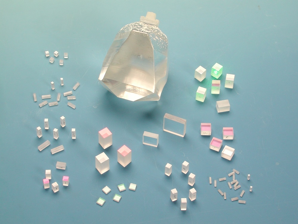
Coupletech Co., Ltd., manufactures, develops and markets a variety of optical crystals which are widely used in the field of optoelectronics, Coupletech product line consists of all kinds of crystal: laser crystals including Nd:YVO4, Nd:YAG, Diffusion Bonded Composite Crystal, Cr:YAG, Nd:YLF etc.; Nonlinear optical ( NLO ) crystals, including KTP, KTA, BIBO, LBO, BBO, DKDP, KDP, LiNbO3 crystal, etc.; Fluoride crystals including CaF2, BaF2, MgF2; Periodically poled crystals: PPLN crystal, MgO:PPLN crystal. We combine high and strict quality manufacturing to supply our products at the most attractive price. We also provide Ti: Sapphire, TGG, AGS, ZGP and other crystals for laser and telecom industries.
Coupletech's Optical Crystal combined with our wide experience and deep technology, we are able to deliver the optimum solution for your applications. We are flexible in customized products and features in high surface accuracy, high surface quality, high flatness. We are also well experienced in the high laser damage threshold AR coatings and HR coatings.
Optical Crystal
Optical Crystal,Laser Crystal,Nonlinear Optical Crystal,Magneto-Optic Crystal
Coupletech Co., Ltd. , https://www.coupletech.com