Note: The wm tool introduced in Android 4.3
Wm command and usage:
instructions:Usage: wm [subcommand] [opTIons]
Wm size [reset|WxH]
Wm density [reset|DENSITY]
Wm overscan [reset|LEFT, TOP, RIGHT, BOTTOM]
Wm size: return or override display size.
Wm density: override display density.
Wm overscan: set overscan area for display.
Explanation: wm is a command for setting the resolution, pixel density, and display area of ​​the mobile phone under the Qualcomm platform (the command similar to the MTK platform is am, other platforms are not touched, not too clear). The parameters are relatively small. The following describes the usage of the command one by one.
1, wm size [reset|WxH]Within [] is optional. Simply running the wm size command will get the display resolution set by lcd itself. As shown below:

The wm size W x H command sets the resolution by witch x hight. If the resolution is set too large, the icon will become larger, otherwise it will become smaller. After setting the resolution, execute the wm size command to see the resolution of the LCD itself and the resolution of overwrite. As shown below:

The wm size reset command sets the resolution to the LCD native resolution.
2, wm density [reset|DENSITY]The usage of this command is similar to the wm size command, which is used to read, set, or reset the LCD's density value. The density value is the ppi of the LCD.
3, wm overscan [reset|LEFT, TOP, RIGHT, BOTTOM]This command is used to set and reset the display area of ​​the LCD. The four parameters are the number of pixels showing the edge distance from the left, top, right, and bottom of the LCD. For example, for a screen with a resolution of 540x960, the display area can be limited to a 540x540 rectangle by executing the command wm overscan 0,0,0,420.
Knowing wm can solve the problem that the LCD icon size is not normal. But these settings are temporary and are suitable for debugging to identify problems and workarounds. For permanent modifications, you can refer to the following two methods (both under the Qualcomm platform):
Method 1: 2" adb root / / prompt read only filysystem execute this command to obtain root privileges,Adb remount
Adb pull /system/build.prop D:\
Add a line at the end of build.prop to ro.sf.lcd_density=240
Adb push D:\build.prop /system/
Adb shell
Cd /system/
Chmod 644 build.prop does not modify the permissions will cause the phone to not come
Method 2: Directly modify system.propY:\xxxx\device\qcom\xxxx\system.prop
Ro.sf.lcd_density=240 Change this value and recompile system.img
How does the LCD electrode reading see the interface technology of the microcontroller?Picking up the measured signal through the measuring instrument is a commonly used data acquisition method in the forward channel design of the single chip microcomputer. Usually, the interface circuit obtains the relevant analog signal from the instrument circuit, and sends it to the single-chip microcomputer through A/D conversion or V/F conversion; or obtains a frequency signal, which is sent to the single-chip microcomputer after being shaped. However, such signals may not be found in some meter circuits. Taking a capacitive pressure sensor sphygmomanometer as an example, although a frequency signal linearly related to the pressure can be obtained from the oscillating circuit and sent to the single-chip microcomputer to measure the pressure, the pressure is not the systolic pressure, diastolic pressure and heart rate to be picked up. The ordinary sphygmomanometer does not have a communication interface like a smart meter to communicate with the microcontroller. Obviously, in order to pick up the signal under test through such a meter, only the reading of its display screen is directly read.
This article takes an automatic sphygmomanometer as an example to introduce the interface circuit for reading the LCD display reading into the MCU. The sphygmomanometer display is a 61/2-segment LCD display with 3 digits showing systolic pressure and 3 digits showing diastolic pressure. The l/2 bit is in the middle of the two sets of numbers and displays four indicators.
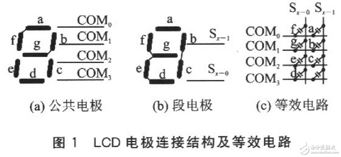
1 LCD electrode connection structure and working waveform 1.1 LCD electrode connection structure1 is an electrode connection structure and an equivalent circuit of a sphygmomanometer LCD. 1(a) is a common electrode connection arrangement, and FIG. 1(b) is a segment electrode connection arrangement. It has 4 common electrodes COM0~COM3, each of which has 2 segment electrodes Sx-0, Sx-1, and its equivalent circuit is a matrix of 4 rows & TImes; 2 columns, as shown in Figure l(c) .
Observe the working waveform of the sphygmomanometer LCD with a dual trace oscilloscope, as shown in Figure 2. It is driven by the time division drive method, with a ratio of 1/3, a duty ratio of l/4, and a B type. The signal waveforms of the common electrodes COM0 to COM3 are always kept constant, and the waveforms of the segment electrodes Sx-0 and Sx-1 vary with the display number. The Sx-1 and Sx-1 waveforms in Fig. 2 are the operating waveforms when the number "O" is displayed.
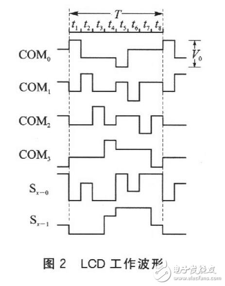
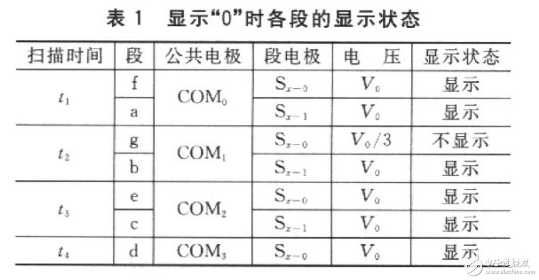
As can be seen from FIG. 2, regardless of the DC component of the signal, the first half periods t1 to t4 of all the waveforms are equal in magnitude to the second half period t5 to t8, and the polarities are opposite. The signal voltages of COM0 to COM3 sequentially reach peak values ​​in four times from t1 to t4. The time t1 is the scanning time of the two segments f and a on the first row, the common electrodes COM0, Sx-0 are segment electrodes of the f segment, and Sx-1 is the segment electrode of the segment a. During the time t1, the voltage COM0-Sx-0=V0 on the f-segment, the voltage COM0-Sx-1=V0 on the a-segment, both f and a are in the selected state and displayed. The voltages and display states of the remaining segments during their scan time are listed in Table 1. In the 7-segment, only the voltage on the g segment is V0/3, which is in the non-selected state and is not displayed. The remaining 6 segments are in the selected state and displayed. Therefore, the number "O" is displayed.
It can be seen that the voltage COMx-Sx-y (x=0,1,...,6;y) on each segment of f, a, g, b, e, c, and d in four times t1 to t4 is sequentially checked. =O,1) Whether it is V0 or V0/3, the glyph codes of the LCD digits can be obtained, and then the glyph codes are converted into measurement results.
2 single chip reading interface circuitFigure 3 is an 805l single-chip reading interface circuit designed according to the above working principle. In the figure, the LCD is a liquid crystal display of a sphygmomanometer. The 6-digit numbers are numbered O~5 from right to left, and the middle half is numbered 6. It has 13 segment electrodes, 4 COM electrodes, and GND is the ground terminal of the sphygmomanometer. The PC port of the 805l is an extended parallel port of the 805l.
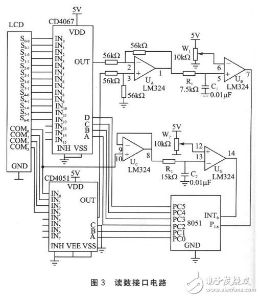
The display state reading circuit is composed of CD4067, CD3405l, LM324 (UA, UB), and the display state of each segment of the LCD digital is read. The CD41367 multi-channel analog switch selects one Sx-x output from the 13 segment electrode signals of the LCD to the inverting input terminal 2 of the LM324 (UA). The CD405l multi-channel analog switch selects one COMx output from the four COM signals of the LCD to the non-inverting input terminal 3 of the LM321 (UA). The LM324 (UA) is connected to the analog subtractor, and the signal COMx-Sx-x is output by the 1-pin. UB is used as a voltage comparator. The reference voltage VR is adjusted by potentiometer W1 between V0/3 and V0, and the segment voltage COMx-Sx-x is compared with VR. The comparison result is the display state of the segment, the high level indicates the segment display, and the low level is not displayed. The display status is fed into the P1.6 pin of the 8051. R1 and C1 form an RC filter to filter out high frequency interference.
For example, to read the display state of the a-segment of the 0th digit, as shown in Fig. 1, the segment electrode of the digital a segment of the 0th is S0-1, and the common electrode is COM0. It is controlled by the program to make PC1PC0=00 in t1 time, make CD405l select COM0, make PC5~PC2=0001, make CD4067 select S0-1, COM0 and S0-1 signal voltages are subtracted by UA subtractor, then UB After the voltage comparison, the display state of the a segment is obtained, and the 8051 reads the most displayed state from the P1.6 pin.
2.2 INT0 interrupt signal generation circuitUC and UD form an INT0 interrupt signal generation circuit. The UC is connected to a voltage follower to reduce the effect of the circuit on the COM0 signal. R2 and C2 form an RC filter to filter out high frequency interference. UD is used as a voltage comparator, the reference voltage VR is added to the non-inverting input terminal, and the VR size is adjusted by the potentiometer W2 to 2V0/3 to V0. The voltage comparator converts the COM0 signal into an INT0 negative pulse signal, and the operating waveform is as shown in FIG. The falling edge of the negative pulse is the start time of the LCD drive signal period T. This negative pulse is connected to the INT0 pin of the 8051, which generates an external interrupt 0 on the falling edge of the negative pulse.

Enable external interrupt 0 and timer T0 to read the glyph codes of the LCD digits in interrupt mode. The main program reads the glyph code by query, and then converts the glyph code into a reading after the reading check, the glyph code to the BCD code decoding, the reading recognition, and the like.
3.1 Read glyph codeThe glyph code of a certain number of LCD is read in an interrupt manner by the external interrupt O and the timer T0. As shown in Figure 5, the INT0 negative pulse causes an external interrupt O at the beginning of the period T, and the T0 timer is started by the INT0 interrupt service routine, f, a, g, b, e in the half cycle from t1 to t4. Each of c, d generates a T0 interrupt, reads the display state of each segment, and obtains a glyph code. The T0 timer is set to the operating mode 2, the automatic reloading timing is T/16, and the initial timing is T/32. The INT0 and T0 interrupt service program flow is shown in Figure 6.
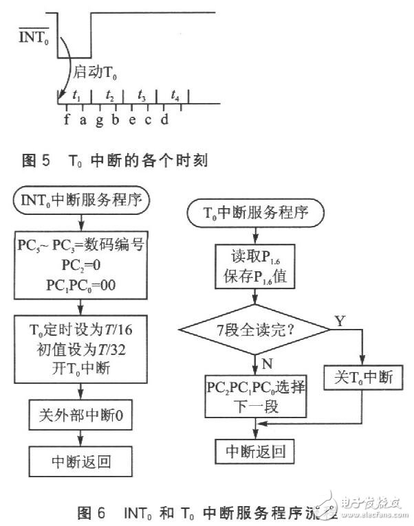
Among them, PC port data format: PC5 ~ PC3 is the LCD digital number to be read, PC2 is the segment electrode number, PC1PC0 is the COM electrode number.
3.2 font code conversionThe main program reads the glyph codes of the digits collected by the interrupt service program in a query manner, and the table table converts the glyph codes into BCD codes, and then converts the digital BCD codes into numerical values.
3.3 Reading verificationIt takes 1 cycle T to read a digital glyph code (actually only the first half cycle), measured, T = 16.318 ms. It takes at least 7 cycles to read all the digits, about 114ms. Taking into account that during the reading of the microcontroller, the LCD reading may change and the reading is wrong. The program uses two consecutive readings to verify the correctness of the reading. If the two consecutive readings are the same, the reading is correct; if the two consecutive readings are different, the reading may be wrong and should be read again.
3.4 Reading recognitionIn addition to systolic blood pressure, diastolic blood pressure and heart rate, the sphygmomanometer also has instantaneous pressure during inflation and deflation, as well as some status information. The half (6th) in the middle of the LCD is used to display the four symbols of Reay to measure, CUFF Inf1aTIng, CUFF DeflaTIng, and Replace Battcries. In addition, when the number 4 is displayed as "E", the measurement error is displayed. When "P" is displayed, the number displayed on the right 3 digits (0 to 2) is the heart rate. When the content on both the left and the right is a number, the left 3 digits (3 to 5) are systolic blood pressure, and the right 3 digits are diastolic pressure. Blood pressure and heart rate alternate. The main program uses this information to identify what the LCD displays.
4 ConclusionUse this interface circuit to collect data without having to consider the details and specifications associated with the measurement of the picked up signal. Thus, when the measurement of the pickup signal is complicated, the development cycle can be effectively shortened. At the same time, it does not have the problem that the data collected by the single-chip microcomputer and the meter reading are not completely consistent in the secondary A/D conversion or V/F conversion method.
The program design reads a 1-digit number with one drive signal cycle. This read speed is sufficient for a sphygmomanometer whose reading changes are not very fast. If the LCD reading of the measuring instrument changes rapidly, you can modify the programming, read several digits simultaneously in one cycle, or even modify the circuit design, and use the second half cycle for reading, so that all the signals are read in one signal cycle. Digital.
Twinkle System Technology Co Ltd , https://www.pickingbylight.com