Low-Voltage Differential Signaling (LVDS) has been proven in a wide range of applications. LVDS offers other advantages while delivering high data rate signals: compatibility with low supply voltages; low power consumption; low emissions; high immunity to interference; Simple wiring and terminal matching.
LVDS is a differential mode (Figure 1). This mode's inherent common-mode rejection provides a high level of immunity to interference. Due to its high signal-to-noise ratio, the signal amplitude can be reduced to approximately 100mV (Figure 2), allowing very High transfer rate. Lower signal swings also help reduce power consumption. Compared with the above advantages, the defect of LVDS (requires two wires for each channel) is already insignificant.
This article refers to the address: http://
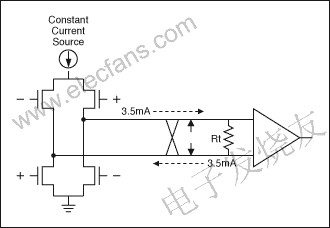
Figure 1. Basic LVDS transmit and receive structure

Figure 2. Signal strength and amplitude of LVDS
With the integration of safety and the increase of auxiliary electronic equipment in the automotive industry, the demand for high-speed interconnection in the automotive field has increased dramatically, mainly for driving support (electronic rearview mirrors, navigation systems, parking distance control, over-the-horizon display). Video display systems, car entertainment systems (television and DVD players), etc. These applications require high-speed data transmission to meet the requirements of image transmission. It is the growth of these demands that has led to the emergence of LVDS products in these areas (Figure 3). 
Figure 3. Typical LVDS connection for automotive applications
LVDS is ideal for automotive applications. There are many sources of electromagnetic radiation inside the car. Therefore, the anti-interference ability is the most basic requirement for automotive electronic design. In addition, considering the low radiation advantage of the LVDS transmission line itself, there is almost no additional interference to other facilities of the system. LVDS transmission requires only a simple resistor connection, which simplifies the circuit layout and makes the line connection very simple (using a twisted pair copper cable). LVDS is compatible with a variety of bus topologies: point-to-point topology (one transmitter, one receiver); multi-drop topology (one transmitter, multiple receivers); multi-point topology (multiple transmitters, multiple receivers)
There is a key problem in automotive design, that is, the ground potential of different positions of the car body is very different, and the potential difference may reach several volts. In a DC-coupled interface configuration, such a potential difference can quickly interrupt data transfer. This problem can be solved by capacitively coupling the signal, provided that the capacitor does not charge the capacitor in the same direction for a long time.
However, the actual application cannot eliminate the possibility of long-term charging in the same direction, for example, when transmitting a long string of consecutive 1 signals. The MAX9213/9214 (Figure 4) avoids these problems with the "DC Balance" technique, which monitors its transmitted data. When displaying a long continuous 1 or 0 signal, the chip flips the data before sending the data. The receiver can easily reconstruct the original signal by flipping the signal. These operations eliminate long strings of consecutive 1 or continuous 0 signals, reducing the effects of capacitive charging, thus effectively solving the ground potential deviation problem. 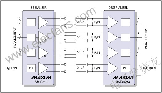
Figure 4. Two-chip transmission scheme that combines transceiver functions with serial-deserialization
Another potential problem can be seen in Figure 3: Numerous system interconnections mean a large number of cable connections, and cable (harness) connections are already very crowded in the original car design. To solve this problem, different data needs to be distinguished. Transmission requirements, not all connections require a particularly high rate, Maxim's MAX9217/9218 can provide up to 700Mbps data rate through a pair of twisted pairs (). With this capacity, a 480 x 800 resolution display can be connected effortlessly. 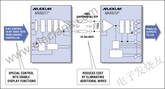
Figure 5. Functional block diagram of the AC-coupled serializer and deserializer
To further optimize electromagnetic radiation characteristics, Maxim's chip also synchronizes all switching operations in the parallel data display to the clock frequency, which can be adjusted from 3MHz to 35MHz (for a given application, the lowest allowed clock frequency) To minimize electromagnetic radiation). In addition, by reducing the amount of switching caused by the data stream itself, including common coding and serial output common mode filtering, it also helps to improve electromagnetic compatibility. Fiber optic interfaces can also improve EMI, but this solution has other problems and is expensive.
LVDS devices must have high ESD protection, especially for input and output pins, which is a very common requirement in the automotive industry. These pins must be capable of withstanding ±15kV air gap discharge, ±8kV contact discharge as specified by IEC 61000-4-2, or ±25kV air gap discharge as specified in ISO 10605, and ±8kV contact protection.
In summary, the LVDS interface is an excellent choice for connecting board-level systems in automotive applications, both now and in the future. In order to achieve this goal, Maxim has developed increasingly sophisticated chips based on the experience of testing and application of the first generation of LVDS products. In recent years, these chips will become the leading LVDS connection solutions in the design of automotive bus systems. product.
10W fast charging model: Using QC2.0/QC3.0 adapter(9V,1.67A) is ONLY for
-Samsung Galaxy S9/ S9plus/ S8/ S8plus
-Samsung Galaxy S7/ S7 edge/ S6 edge plus/ Note 5
SLEEP-FRIENDLY:Sleep-friendly blue LED charge status light lets you charge phone at night without keeping the family awake.Keeping your confortable sleeping.
Lightweight & Ultra-Thin:Portable and Antislip rubber strip keeps any phone in place to ensure complete security while charging. Sleek and compact build takes up minimal space with 0.38in thickness.
Case Friendly:The sensor is sensitive and can be recharged through the casing, 8mm induction distance, the case can be recharged by the case, without affecting the charging speed (Sensing distance<8mm)
Qi Certified Safe:Overvoltage protection, temperature control, quick acting charging , the built-in foreign boby monitoring function can intelligently identify the charging device
10W Quick Wireless Charger For All Qi enabled Phones
10W Wireless Charger,Wireless 10W Fast Charging Pad Stand,Ultra-Slim Wireless 10W Charger
Shenzhen Kantou IM Technology Co., Ltd. , http://www.kantou-im.com