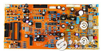
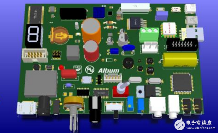
Proper layout of PCB components in chip processing is the basic premise for designing high quality PCB patterns. The requirements for component layout mainly include five aspects of installation, stress, heat, signal and appearance.
Refers to a series of basic requirements for the installation of the board into the chassis, the enclosure, and the slot in a specific application without causing interference such as space interference or short circuit, and placing the specified connector in a specified position on the chassis or the casing. Claim.
The circuit board in the chip processing should be able to withstand various external forces and vibrations during installation and operation. For this reason, the circuit board should have a reasonable shape, and the positions of various holes (screw holes, shaped holes) on the board should be reasonably arranged. Generally, the distance between the hole and the edge of the plate is at least greater than the diameter of the hole. At the same time, it should be noted that the weakest section of the plate caused by the shaped hole should also have sufficient bending strength. The connector that directly “extends†the device from the board should be reasonably fixed to ensure the reliability of long-term use.
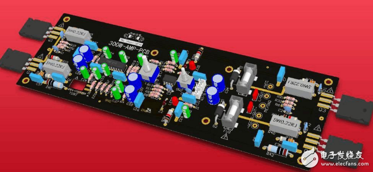
For high-power, severely heated devices, besides ensuring heat dissipation conditions, be careful to place them in the proper position. Especially in sophisticated analog systems, special attention should be paid to the adverse effects of the temperature field generated by these devices on the fragile preamplifier circuit. Generally, the part with very large power should be made into a single module and take certain thermal isolation measures from the signal processing circuit.
Signal interference The most important factor to consider in PCB layout design. The most basic aspects are: weak signal circuit and strong signal circuit are separated or even isolated; AC part is separated from DC part; high frequency part is separated from low frequency part; pay attention to the direction of signal line; ground line arrangement; proper shielding and filtering And other measures.
5, beautifulNot only must we consider the neatness of the placement of components, but also consider the graceful flow of the traces. Since the average layman sometimes emphasizes the former, to evaluate the advantages and disadvantages of the circuit design one-sidedly, for the image of the product, the former should be given priority when the performance requirements are not critical. However, in high-performance applications, if you have to use a double-panel, and the board is also packaged inside, you can't see it normally, you should give priority to the aesthetics of the trace.
| About Film Covered Wire |
Glass-fiber covered polyester film covered rectangular copper (aluminium) wire .includings Glass-fiber Polyimide Film Covered flat Copper wire, Glass-fiber Polyimide Film Covered flat Aluminium wire, Glass-fiber Polyester Film Covered flat Copper wire, Glass-fiber Polyester Film Covered flat Aluminium wire, Glass-fiber Covered flat Copper wire, Glass-fiber Covered flat Aluminium wire.
Packaging of Products
30/50/150 kg wooden spool
Application: medium and large electrical motor and transformer windings

Aluminium Wire,Film Covered Wire,Polyimide Film Covered Copper Wire,Film Covered Flat Wire
HENAN HUAYANG ELECTRICAL TECHNOLOGY GROUP CO.,LTD , https://www.huaonwire.com