1 Introduction
Digital Signal Processor (DSP) is a microprocessor suitable for implementing various digital signal processing operations. It has the following main structural features: (1) Improved Harvard architecture with independent program bus and data bus The instruction and data space can be accessed at the same time, allowing actual transfer between the program memory and the data memory; (2) support pipeline processing, the processor divides the operation of each instruction into several stages of instruction fetching, decoding, and execution. At the same time, several instructions are processed at different stages at the same time; (3) the chip contains a special hardware multiplier, so that the multiplication can be completed in a single cycle; (4) the special instruction structure and addressing mode satisfy Digital signal processing FFT, convolution and other operational requirements; (5) fast instruction cycle, can process tens of millions or even hundreds of millions of fixed-point or floating-point operations in each second; (6) mostly set up a separate DMA The bus and its controller can perform high-speed parallel data transfer without affecting the speed of digital signal processing.
A complete control system can be constructed by a DSP plus memory, analog-to-digital conversion unit and peripheral interface, but it is not feasible to achieve high-speed real-time control. Because a real-time control system generally needs to complete tasks such as data acquisition, analog-to-digital conversion, analysis and calculation, digital/analog conversion, real-time process control, and display, relying on a single DSP to complete these tasks will inevitably greatly extend the control of the control object. Cycles that affect the performance of the entire system. So we add a CPU that is responsible for tasks such as data acquisition, analog-to-digital conversion, process control, and human-machine interface, so that DSP can focus on the implementation of system control algorithms and make full use of its high-speed data processing capabilities. From the perspective of performance and price ratio, this CPU uses an 8-bit 51 series microcontroller. At this time, data sharing between the two CPUs becomes an important issue.
The use of dual-port RAM (referred to as DRAM) is an effective way to solve data sharing between CPUs. Compared with serial communication, the dual-port RAM not only has high data transmission speed, but also has good anti-interference performance. In the power active filter developed by the author's laboratory, TI's third-generation DSP chip TMS320C32 and 51 series single-chip microcomputer 89C52 were selected as the CPU of the control system. The data exchange is completed between the two CPUs through the dual port RAMCY7C133. However, in the actual use process, the problem that the 89C52 and the dual port RAM bus width do not match is encountered, and the design of the interface circuit is required.
2 dual port RAMCY7C133 internal structure and function
CY7C133 is a high-speed 2K & TImes; 16CMOS dual-port static RAM developed by CYPRESS. It has two independent, fully symmetrical address buses, data buses and control buses. It is available in a 68-pin PLCC package with a maximum access time of 25/35/55ns. . The master-slave mode makes it easy to expand the data bus to 32 bits or more. The function of each pin is shown in Table 1. The internal functional block diagram is shown in Figure 1.

CY7C133 allows two CPUs to read any memory location at the same time (including reading the same address location at the same time), but it is not allowed to write or read the same address location at the same time, otherwise an error will occur. The arbitration logic (busy logic) circuit is introduced in the dual-port RAM to solve this problem: when the left and right ports are simultaneously written or read and written to the same address unit, the stable address port is preferentially read and written by the arbitration logic circuit, and the internal The circuit validates the signal of the other port and internally disables access by the other party until the end of the port operation. The BUSY signal can be used as an interrupt source to indicate that this operation is illegal. In the master-slave mode, the signal of the master chip is connected to the pull-up resistor as an output, and the signal from the chip is used as a write disable input.
Interface circuit between 3DSP, single chip microcomputer and dual port RAM
The address bus width of the 89C52 is 16 bits, and the data bus is 8 bits. The data bus width of the TMS320C32 is 32 bits, and the address bus width is 24 bits. The data bus width of CY7C133 is 16 bits, and the address bus width is 11 bits. Therefore, the interface between TMS320C32 and dual port RAM is nothing special, but the interface circuit between 89C52 and dual port RAM needs to expand the bus to 89C52. It is. The specific method is to use the latch function of the latch 74HC373 to realize time-sharing reading and writing by controlling the enable signal, thereby realizing the expansion of the data bus, that is, using the latch as the virtual bus. The specific read and write processes, read and write signals, and latch enable signals will be described in detail below. The interface circuit between DSP, MCU and dual port RAM is shown in Figure 2.
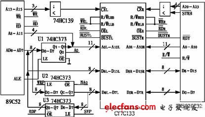
The address space allocated by the TMS320C32 to the dual port RAM is 0x800000h~0x8007FFh. The A20 to A23 and the STRB are decoded by the 38 decoder 138, and the chip select signal CER of the dual port RAM is given. The address space allocated by the 89C52 to the dual port RAM is 0x1000h to 0x1FFFh. The A13 to A15 are decoded by the 24th decoder 74HC139 to generate the chip select signal CEL of the dual port RAM. The dual-port RAM has two read/write control signals on each side to control the read/write of the upper byte and the lower byte respectively. When used, the upper and lower bits of the data can be written separately as needed. In the interface circuit shown in Figure 2, the two read/write control signals on both sides are connected together, that is to say, the read and write of the dual-port RAM is simultaneous reading and writing of 16-bit data.
The read/write signal of the dual port RAMCY7C133 and the enable signal of the latch 74HC373 in Fig. 2 are shown in Fig. 3. Among them, WR is the write control signal of 89C52, RD is the read control signal of 89C52, A0 is the lowest address of 89C52, A15 is the highest address of address, R/W is the read/write control signal of TMS320C32, BUSYL is connected with P1 of 89C52 One pin (specifically, it can be selected according to the actual situation of the system, not shown in the figure), BUSYR is connected to the READY signal of TMS320C32.

Let's discuss the 89C52's read and write process for dual-port RAM. When the 89C52 reads data to the dual-port RAM, it can be seen from Fig. 3 that A0 should be low at this time, and it is assumed that the address is 0x1000h, and the 16-bit data stored at the address in the dual-port RAM is simultaneously read out due to The upper 8-bit data line is directly connected to the 89C52 8-bit data line, so the upper 8 bits of data are immediately read into the 89C52. At the same time, according to the mutual logic relationship of the signals in Fig. 3, it is not difficult to judge that the enable signal LE of U3 is valid (high level), OE is invalid (low level), and thus the lower 8 bits of data are sent into U3 and latched. . Then 89C52 performs another read operation. At this time, the address becomes 0x1001h. Since A0 becomes high level, the read enable signal of the dual port RAM becomes an inactive level, so this read operation has no effect on the dual port RAM. Looking at the changes in the enable signals LE and OE of U3, it is clear that LE becomes an inactive level, and OE becomes the active level, the last latched data (ie, the lower 8 bits of the dual port RAM) Was sent to 89C52. When the 89C52 writes to the dual-port RAM, note that A0 should be high at this time. It is assumed that the address is 0x100Ch. It can also be judged according to Figure 3 that the enable signals LE and OE of U2 are active levels, so the data It is simultaneously written into the dual-port RAM (that is, the high 8-bit data of the dual-port RAM is the same as the lower 8 bits at this time); then the 89C52 performs another write operation, and the address becomes 0x100Dh, because A0 becomes low level. The chip of U2 is selected as the inactive level, U2 is blocked, and the data is written to the upper 8 bits of the dual port RAM. From the above analysis, the 89C52 successfully reads or writes data in the dual-port RAM by two consecutive read or write operations using the different levels of the lowest address bit A0, but only when reading in. The upper 8 bits are read, and the lower 8 bits are read. The write is written to the lower 8 bits and then to the upper 8 bits.
4 software implementation
Dual-port RAM must use a certain mechanism to coordinate the read and write operations of the CPU on the left and right sides, otherwise there will be errors in reading and writing data. The two sides can usually be coordinated by interrupt, hardware, token and software. This article uses software. From the above analysis, we can know that the interface address circuit has actually used the lowest address bit A0 of 89C52 to divide the storage space of the dual port RAM into two spaces of odd and even addresses. Among them, the odd address space is dedicated to 89C52 write, and the even address space is reserved for 89C52. Then we only need to deal with the software of TMS320C32, that is, TMS320C32 is read-only for the odd address space of dual-port RAM, and only writes to the dual address space. This avoids the TMS320C32 and 89C52 writing to the same address unit of the dual port RAM. In addition, before accessing the dual-port RAM, the CPU first queries the BUSY signal of the local end, and only reads and writes when the local/BUSY signal is invalid, further ensuring the reliability of data reading and writing.
5 Conclusion
The data communication between the dual CPUs is realized by the dual port RAM, which greatly improves the data transmission speed and reliability, and satisfies the real-time and high-speed control requirements of the control system. The interface circuit between 89C52 and dual-port RAM designed in this paper is simple and practical, and successfully solves the problem of bus matching. It also has certain reference value for other systems that need bus expansion.
Bright White Candles/velas/bougies .make of paraffin wax ,and stearic acid .
snow white and pure white color ,very bright quality holy brand candles .happy candles .OEM brand .
usually yellow color box packing ,red color box packing this packing more popular aslo the box can add shrink paper pack ,and 35g/pc 8x30box/ctn 36g /pc /
if any inquire pls tell me exact weight ,then I will offer you best price .welcome to visit my factory
and shipment in the 30days after get the depsoit .
Bright Candle,Bright Different Colors Candle,Bright Birthday Candle,Ultra Bright Led Candle
Shijiazhuang Zhongya Candle Co,. Ltd. , https://www.zycandlefactory.com