1 Overview
This article refers to the address: http://
The main data of the tachograph includes accident suspects and driving status data. The accident suspect data is that the recorder continuously records and stores the vehicle traveling speed and the vehicle braking state signal corresponding to the real time of 20 s before the parking at a time interval of not more than 0.2 s, and the number of recordings is at least 10 times: the driving state data is The vehicle travel speed information corresponding to the real time is provided by the recorder regardless of whether the vehicle is in a running state or a stopped state. The recorder shall be capable of continuously recording and storing the driving state data of the vehicle within the last 360 hours at intervals not exceeding 1 min, which is mainly the average per minute interval corresponding to the real-time time of the vehicle during driving. Travel speed value [1].
The recorder requires a large-capacity data storage. Previous designs have used parallel or ferroelectric memories. Among them, the parallel memory has a large storage capacity and a fast read/write speed. However, the anti-interference ability is poor, and the interference on the car is strong. Although it can be avoided by other software and hardware measures. However, in design, it is generally necessary to select a chip with strong anti-interference ability; the ferroelectric memory uses a serial interface, which has strong anti-interference ability and high flexibility, and can be read and written in a single byte (no need to erase, directly Rewriting the data), but its storage density is small, the unit cost is high, and the reading and writing speed is slow. Since the tachograph requires the speed and state to be sampled every 0.2 s, the speed of reading and writing the memory affects the sampling accuracy and the operation of the program.
The current EEPROM flash memory array Flash Memory has ATMEL, SST's Small Sector Flash Memory and ATMEL's Data-Flash Memory. These devices have the combined advantages of EEPROM and NOR technology Flash Memory, mainly as follows:
(1) The read/write flexibility is worse than EEPROM, and data cannot be directly rewritten. The page erase is required before programming. Compared with the block structure of the NOR technology Flash Memory, the page size is small, and thus has the characteristics of fast random read, fast programming, and fast erase:
(2) Compared with EEPROM, this memory has obvious cost advantages;
(3) Storage density is larger than EEPROM, but smaller than NOR technology Flash Memory [2].
Therefore, the Dataflash has a large storage capacity, a fast reading and writing speed, and strong anti-interference ability, and is a good choice for the memory in the tachograph. This paper presents a recorder design using ATMEL's AT45DB161B to store data.
2 AT45DB161B serial memory
The representative model of ATMEL's Data-Flash products is AT45DBxxxx. This series of memory has a large capacity (from 1 to 256MB); the package size is small, the minimum package type (CBGA) size is 6 mm × 8 mm: SPI interface can be used for reading and writing; less hardware connection; internal page size is smaller The page size of 8 MB capacity is 264 bytes, the page size of 16 MB and 32 MB capacity is 512 bytes, the page size of 64 MB capacity is 1056 bytes, and the page size of 128 MB capacity and 256 MB capacity is 2112 words. Section. In addition, the AT45DBxxxx series memory has two SRAM buffers with the same size as the main memory page, which can improve the flexibility of the system and simplify the data reading and writing process. The operating voltage of the AT45DBxxxx series memory is only 2.7 ~ 3.6 V; the power consumption of the whole chip is also small; the typical read current is 4 mA, the standby current is only 2 μA: the read/write speed is up to 20 Mbps.
The AT45DB161B has a capacity of 16 MB. Divided into 4096 pages, each page has 528 bytes [3]. There are also two 528-byte data buffer SRAMs. The two SRAMs can also receive data while operating on the main memory. Therefore, compared with serial EEP-ROM. This device can greatly reduce the read and write time. Compared with the parallel flash, the SPI bus interface is not slow, and the anti-interference ability is relatively strong.
2.1 AT45DB161B pin interface definition
Table 1 lists some of the interface pin definitions for the AT45DB161B. CS is the chip select signal, RESET is the reset terminal, SCK, SI, SO are the SPI bus, RDY/BUSY is the busy signal, and WP is the first 256 pages of write protection.
The SPI interface is a general-purpose serial interface bus that uses three lines of SCK, SI, and SO for data read/write control. The data is in bytes (8 bits). Among them, SCK is the clock signal, and SI and SO are the data input and output lines.
The AT45DB161B only supports SPI modes 0 and 3. In both modes. The rising edge of the SCK signal triggers the data input, and the falling edge triggers the data output. The difference between the two is that the starting level of SCK is different. When AT45DB161B is reset, the default is SPI mode 3.
2.2 Instructions
In addition to the storage unit, the AT45DB161B internally includes a command user interface (CUI) and a state machine. The CUI receives the user's software instructions to translate it into a state machine internal opcode and performs a validity check of the command. The state machine controls all internal operations of the memory. The device contains an 8-bit status register that can be used to indicate the operational status of the device. The Read Status Register command is input to the memory to read the data of the Status Register. The following briefly describes the read and write memory locations and status register instructions for mode SPI0 and mode SPI3.
(1) Read status register
Send the command word 0XD7. The status word (one byte) can be obtained directly, in the following format:
When RDY/BUSY is 1, it means not busy, and can receive the next instruction; if it is 0, it means busy.
The design can be used to determine whether the previous instruction has been read or written by reading the status register or the SO port. When the memory is not busy, the SO port changes from 0 to 1. In addition, the RDY/BUSY port can also be used to determine if the previous instruction has been read or written.
COMP is used to indicate the comparison result of the data in the main storage unit and the data in the buffer: COMP is 0 to indicate equality. A COMP of 1 indicates a difference. Bit5-Bit2 can represent the size of the memory.
(2) read memory instruction
There are two ways to read the data of the memory, as shown in Figure 1. One of them is to directly read the data of any address of the memory, which can be realized by the instruction D2H plus 3 bytes of Dataflash address plus four bytes of null data. Take SPI mode 3 as an example, its working sequence is shown in Figure 2. Shown.
The other is to read the data of a certain page on the memory through the buffer 1 (2). This method can be divided into two steps: one is to read the data to the data buffer 1 (2), that is, the page address in the 53H (55H) + 3 bytes of Dataflash (in any SCK mode); Read data buffer 1 (2), which can be implemented with instruction D4H (D6H) + 3 byte address (mainly indicating which address of the data buffer to start reading) + 1 byte of empty data.
(3) write data to the memory
There are also two modes for writing memory, as shown in Figure 4. One of them is written directly to the memory through buffer 1 (2); the other is to write to the buffer first, and then write the data of the buffer to the memory.
The format of the above commands is a one-byte command + 3 bytes of address.
3 W77E58 and AT45DB161B interface circuit
W77E58 is a high-speed enhanced version of WinBond: MCS-51 series MCU. The system using the W77E58 is 2.5 times faster than the traditional 51 series. The W77E58 operating at 40 MHz is equivalent to the 80 MHz 8051, plus its built-in 32 KB reprogrammable Flash EPROM and 1 KB internal SRAM accessed with MOV instructions (saving 16 data/address I/O lines). And 2 enhanced full-duplex serial ports and lower price, W77E58 is undoubtedly a high-performance, multi-functional, highly integrated 8-bit microcontroller, ideal for high-speed, dual serial ports, simple and low-cost peripherals system. Its anti-interference performance and encryption performance are relatively good [4].
4 software implementation
Since the W77E58 does not have an SPI bus, it needs to be implemented in software. The SPI bus emulation program and the AT45DB161B read and write program are given below.
The software is programmed with Keil C and its source code is as follows:
4.1 SPI bus simulation
(1) Read a byte from the SPI
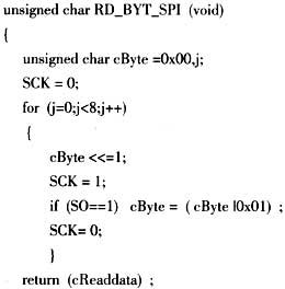
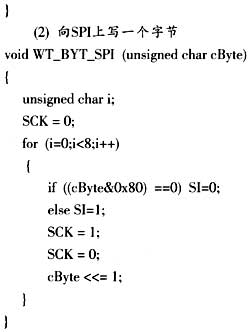
(2) write data in Datanash
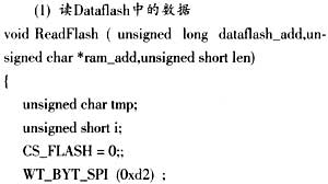
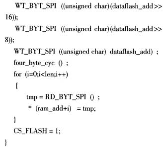
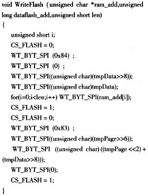
The following program stores data by first writing to the buffer and then writing the buffer's data to memory:
Single Burner Electric Hotplate
Portable Hot Plate,Single Burner Electric Hotplate,Hot Plates,Hot Plates With Stainless Housing
Shaoxing Haoda Electrical Appliance Co.,Ltd , https://www.hotplates.nl