Digital signal microprocessor DSP has the functions of high-speed operation and data processing. It provides an effective hardware platform for the mathematical calculation of real-time navigation system with its high performance and low power consumption. In modern weaponry, a car navigation system based on DSP chip is designed, which plays an important role in civil and military fields. The system has high reliability and security.
1 How does the car navigation system work?
The main function of the car navigation system is to regularly collect the gyro orthogonal coded signal, the accelerometer input and the odometer input signal, and perform necessary processing on the collected data to realize the navigation solution. At the same time, the collected data is sent to the ground monitoring device through the RS422 bus and the CAN bus; and the relevant commands and parameters are received through the RS422 bus. The structure of the system is shown in Figure 1.
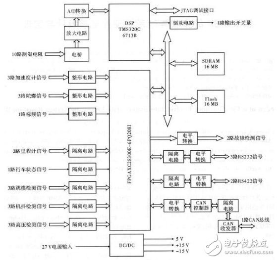
Figure 1 Block diagram of the car navigation system
2 system hardware design
2.1 processor and memory design
The car navigation system circuit uses TI's TMS320C6713B-A200 as the DSP. The DSP chip has a nominal frequency of 200 MHz, and the DSP processing capability is 1600 MI·s-1/1 200 MFLOPS when operating at 160 MHz. Using a 40 MHz crystal oscillator as the clock input of the DSP, it is used as the clock for DSP operation after being multiplied by the internal phase-locked loop. It uses a TPS70345 voltage regulator to provide 3.3 V IO voltage and 1.2 V core voltage. The 16 MB MT48LC4M3282TG-7IT chip is used as the memory of the SDRAM. The memory is directly connected to the EMIF bus of the DSP. The address lines BA1, BA0 and A11~A0 of the SDRAM chip are connected to the EA15~EA2 of the DSP chip, and the data lines D31~D0 are connected to the ED31~. ED0. The address line A22~A0 of the FlashRom chip is connected to the GP13~CP11 and EA21~EA2 of the DSP chip, the data line DQ15~DQ0, and the ED15~ED0. The state of the GP13~GP13 pins is high during initialization, and the chip select signal of the SDRAM chip Connected to the CE0 of the DSP chip; a S29GL128N10TFIR1 chip with a capacity of 16 MB is used as the FlashRom memory, and the chip select signal of the FlashRom chip is connected to the CE1 of the DSP chip. The reason why the DSP chip's CE1 is connected to the FlashRom chip is because the boot mode is loaded from the ROM, and the BOOT program is stored in the FlashRom memory. The read and write signals of the memory are all connected to the AWE signal of the DSP chip. The DSP accesses the external memory through the EMIF bus interface, and the access to the external memory can be controlled by operating the registers, simplifying the circuit design.
2.2 Power supply design
The car navigation system input power is 27±9 V, and the MHF+28515 converts 24 V to +15 V and +5 V. The MHF+28515 has an input voltage range of 16~48 V and an output power of 15 W. The 5 V voltage output has a maximum power of 7.5 W, a current of 1 500 mA, and a maximum output power of +15 V for 5 W and a circuit of 330 mA. Since the current of the +5 V power supply of the car navigation system circuit is about 1000 mA, it can provide +5 V, current "140 mA output for external use. In order to meet the power supply requirements of various components in the system, a car navigation system is designed. power supply system.
The +5 V power supply of the MHF+28515 provides digital power for the entire module. The +5 V chip that is used by the CAN bus protocol chip directly uses the power supply. Other circuits use the converted power supply. The processing methods include: voltage adjustment. The TPS70345 converts the +5 V supply to a 3.3 V and 1.2 V supply, of which 3.3 V is used for DSP peripheral circuits and SDRAM, Flash, etc., 1.2 V for the DSP core; the +5 V supply is converted to a voltage regulator TPS70351 3.3 V and 1.8 V voltage, 3.3 V for FPGA peripheral circuits, optocouplers and other chips, 1.8 V for FPGA cores; +5 V power supply to 3.3 V voltage through two DC/DC modules NKE0503, one for RS422 The MAX3490 and optocoupler in the isolated circuit are used, and the other is used in the MAX3232 and optocoupler in the RS232 isolation circuit. The +5 V supply is isolated by a DC/DC module NME0505 for use with the MAX481, CAN bus transceivers and optocouplers on its path. The ±15 V supply from the MHF+28515 provides analog power to the entire module. The +15 V voltage is converted to a +5 V analog voltage by the three-terminal regulator JW78M05 for use with the LM3940IMP and REF196; +5 V analog voltage is passed The LM3940IMP is converted to a 3.3 V analog voltage to power the op amp; the +5 V analog voltage is converted to a 3.3 V analog voltage by the REF196 to power the bridge; the +15 V and -15 V voltages are used to power the op amp OP497.
2.3 Input signal
The input signal of the car navigation system circuit has 3 accelerometer signals, 3 gyro signals, two odometer signals, two road sign frequency signals, one road state signal, nine road state detection signals and ten road temperature signals.
The signal form of the accelerometer signal is reversible pulse, amplitude TTL, full-scale 256 kHz, counted by three 16-bit counters, rising edge trigger, interrupt 5 latch, accelerometer signal using RC filter and Schmitt trigger input The inverter is shaped and then introduced into the FPGA after level shifting through the 74LVC244.
The signal form of the gyro signal is orthogonal coded signal, the amplitude is high level 4~5 V, low level is 0~0.8 V, current is ≤8 mA, frequency is ≤1.5 MHz, phase difference is 90°±20°, via 3 way The 16-bit counter counts, the rising edge triggers, the interrupt 5 latches, and the gyro signal is also the same as the accelerometer signal for shaping processing. The frequency of the standard frequency signal is 128 kHz, the amplitude is TTL, and the signal needs to be shaped. Therefore, the processing method of the standard frequency signal is the same as that of the accelerometer signal processing.
The odometer signal includes two odometer signals, one driving status signal and one odometer ground, the amplitude is 12 V, the driving capacity is 30 mA, the optocoupler isolation is required, two 16-bit counters and one bit status register are set, respectively Record the odometer pulse input and status information, the odometer pulse rising edge triggers the count, interrupts 5 latch; requires the driving status signal State to be enabled and disabled by the command, and when the state=1, the odometer signal is added and counted; When State=0, the subtraction counts; the odometer signal is added and counted in the prohibited state, and the odometer signal passes through the RC filter circuit and the protection diode, and then enters the FPGA through the optical isolation.
The state detection signal includes three hopping mode detection signals, three high voltage state signals and three oscillating state signals. The signal forms are all switching quantities, and the amplitude is TTL. The machine sway state signal and the high voltage state signal need to be optocoupler isolated. The processing mode and parameter selection of the mode-detection detection signal are the same as the accelerometer signal; the high-voltage state signal and the machine shake detection signal processing form are identical to the gyro signal.
The temperature measurement signal includes 10 temperature measuring resistance input and 1 temperature measuring resistance input common end, the temperature range is -45~+70 °C, the temperature measuring resistor and the three high precision resistors on the module form a bridge, according to the working principle of the bridge The resistance of the bridge arm resistance should be less than the minimum value of the temperature measuring resistor, and certain redundancy should be considered. The formula for calculating the temperature coefficient is R0&TImes; 3.85 & TImes; 10-3, where R0 is 0 °C resistance, due to the high Precision resistor and 12-bit AD, A / D conversion accuracy "0.5 °C, can be achieved with a multiplexer. The midpoints of the two arms of the bridge are respectively connected to the operational amplifier for follow-up processing, and then the A/D conversion chip collects the temperature test result after the post-stage amplification, and the A/D conversion chip adopts the serial interface chip, and is connected with the McBSP1 interface of the DSP. The chip has a resolution of 12 bits and has a conversion time of 10 μs and a maximum of 11 channels of A/D input.
The CAN bus design is adopted in the circuit design of the car navigation system. The CAN bus independent controller adopts SJA1000T and uses 16MHz crystal as the clock input. The ID number and data transmission baud rate can be configured by software, and the maximum rate is 1 Mbit·s-1. The bus controller uses a data address multiplexing bus and is connected to the DSPEMIF bus after being converted by the FPGA. The CAN bus controller signal uses TTL level (5 V), and the SN74LVC4245 is used for level conversion between the FPGA and the 3.3 V level signal. The CAN bus receiver uses the Philips Semiconductors PCA82C250. The data transmission signals between the bus controller and the transceiver are isolated by optocouplers. The CAN bus interface circuit is shown in Figure 2.
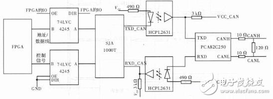
Figure 2 CAN bus interface circuit
2.4 FPGA design
The car navigation system circuit adopts the control logic on the FPGA processing module, the counting of each input signal and realizes the serial interface communication protocol. The FPGA counts the input signal, and divides the standard frequency signal to generate an interrupt 5 signal, and generates an interrupt 5 signal while latching each counter value. The DSP can access the internal resources of the FPGA through the EMIF bus. The address space occupies the loading mode of the CE2.FPGA of the EMIF bus as the Master Serial Mode. The functional block diagram of the FPGA is shown in Figure 3. The FPGA design includes accelerometer signal counter design, gyro signal counter design, odometer signal counter design, gyro frequency counter design, frequency divider design, status detection, fault detection signal and serial communication interface design.
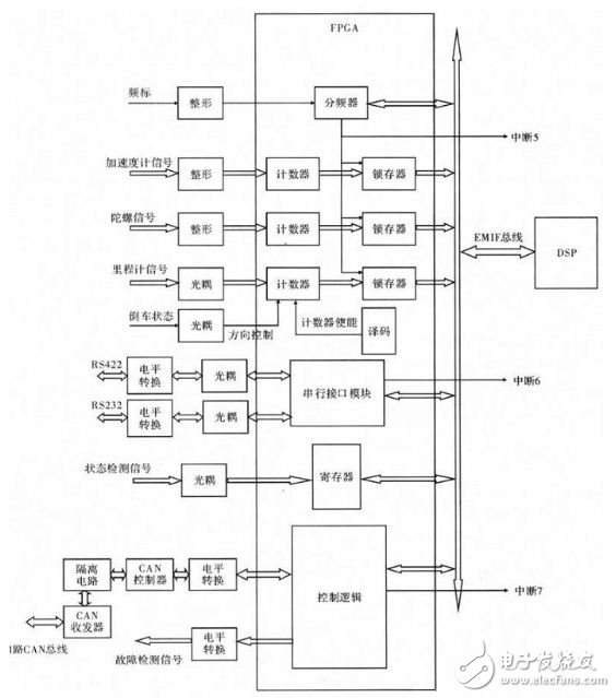
Figure 3 FPGA functional block diagram
The accelerometer signal input is a reversible pulse. Each channel accelerometer input includes 3 signals, which are +A, -A, and GND. According to the design requirements, the count value increases when there is a pulse on the +A signal, and the pulse on the -A signal The time count value is decreased, and when the frequency band frequency division interrupt is generated, the count result is stored in the latch. A 16-bit counter is designed in the FPGA, the power-on reset counter is 0, the count value is increased by 1 when there is a pulse on the +A signal, and the count value is decreased by 1 when there is a pulse on the -A signal. When the frequency division interrupt is generated, The result of the counting is stored in the latch, and the DSP can obtain the result of the accelerometer signal counter through the EMIF access latch.
The gyro signal input form is orthogonal coded signal, and each channel gyro signal input includes 3 channels, which are A, B and DGND respectively. When the A phase leads the B phase by 90°, the count value increases, when the A phase falls behind the B phase by 90°. The time count value decreases. In the design, the input signal first passes through the phase-detection circuit, recognizes the phase sequence of the A-channel and the B-channel signal, and generates two reversible pulse signals of 4 times frequency, and then counts the reversible pulse. When the standard frequency signal is interrupted, The result of the counting is stored in the latch.
The odometer signal includes two counting inputs and one driving status signal input. Each counting input uses a 16-bit counter. When the interrupt is generated, the counter value is stored in the latch; the driving status signal (STATE) is initially powered in an invalid state. The user sets the STATE status to be valid by a command. When the STATE signal is in the active state, the STATE is 1, and the odometer counter counts up; if the STATE is 0, the odometer counter counts down; and when the STATE signal is inactive, the odometer counter increments.
A 16-bit counter is designed in the FPGA. The power-on reset counter is 0, the counter value is increased, and the counter is incremented by 1. When the frequency divider interrupt is generated, the count result is stored in the latch. The DSP can obtain the result of the gyro frequency counter through the EMIF access latch.
The standard frequency divider is used to divide the standard frequency signal to generate a state interrupt signal for latching the acceleration counter, the gyro counter, the odometer counter, and the status detection signal in the FPGA. In the FPGA, the standard frequency divider consists of a prescaler and a counter. The frequency division can be set by software programming. The DSP writes the value to be divided into the prescaler through the EMIF bus. The counter records the number of frequency pulses and counts. When the calibration value is reached, the counter outputs and clears, and the counter outputs an interrupt to the DSP, and simultaneously latches the acceleration counter, the gyro counter, the count value of the odometer counter, and the state of the state detection signal in the FPGA.
The status detection signal is a binary signal, the state is stored in an address, and each bit represents the state of one way. A 16-bit register is designed in the FPGA to store the driving state, the state of the high voltage detection signal, the state of the jitter detection signal, and the state of the mode detection signal, and latch the signal into the latch during the interrupt.
The fault detection signal is written to the fault detection vector through an address. According to the fault detection vector, each bit is specifically 0 or 1. The programmable logic device automatically sets the fault detection vector to the output pin. An 8-bit memory is set in the FPGA to store the fault detection vector, and the signal is driven and output.
The serial protocol module is designed inside the FPGA, and the RS232 and RS422 serial interfaces are formed by the external circuit. The integrated protocol chip is designed with reference to ST16C2552, and its MODEM control and other functions have been reduced. The serial interface operating baud rate can also be set.
3 Conclusion
This paper introduces the DSP-based car navigation system and gives the hardware circuit design. The utility model has the advantages of simple structure, high reliability, convenient maintenance, improved overall performance and cost performance of the system, and good inheritance and the like. Practice has proved that the hardware circuit is reliable and provides a reference for hardware design in the field of car navigation.
Featured by flat surface with measurement 11.5mm width by 21mm height, side bend. This size covers all of our colors and functions including mono, tunable white, RGB, RGBW,DMX and SPI. S15 is the best-selling size among all our models, which are now widely used in high class façade lighting, pool lighting, advertisement and etc.
Bluetooth LED Neon, led neon Bluetooth
Tes Lighting Co,.Ltd. , https://www.neonflexlight.com