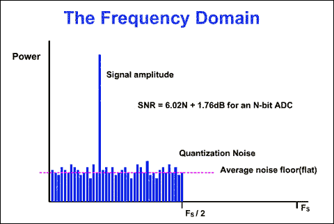
The latest sigma-delta converters typically feature higher resolution, high integration, low power consumption, and lower cost, making them the perfect ADC choice for process control, high precision temperature measurement, and electronic scale applications. But because designers often don't know much about Σ-Δ type converters, they choose traditional SAR ADCs. The analog side of the sigma-delta converter (1-bit ADC) is very simple; the digital side performs filtering and sampling, which is more complicated, which makes the production cost of the sigma-delta ADC lower. To understand how the converter works, you must be familiar with concepts such as oversampling, noise shaping, digital filtering, and sampling. This application note covers the above topics. OversamplingFirst, consider the frequency domain transfer function of a conventional multi-bit ADC when the input signal is a sine wave. The input is sampled at frequency Fs. According to Nyquist's theorem, Fs must be at least twice the bandwidth of the input signal. Looking at the FFT analysis of the digital output, we can see a single tone and a large amount of random noise extending from DC to Fs/2 (Figure 1). These noises are called quantization noise, and the result can be considered as follows: The ADC input is a continuous signal with an infinitely possible state, but the digital output is a discrete function, and the number of different states depends on the resolution of the converter. Therefore, the conversion from analog to digital loses some information and introduces a certain degree of distortion into the signal. The magnitude of this error is random and the maximum is ±LSB.
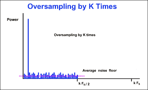
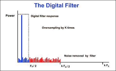
If we divide the fundamental frequency amplitude by the RMS sum of all noise frequencies, we get the signal-to-noise ratio (SNR). For an N-bit ADC, SNR = 6.02N + 1.76dB. In order to increase the SNR of a conventional ADC (and thereby improve the accuracy of signal reproduction), it is necessary to increase the number of bits. Still the above example is an example, but the sampling frequency is increased, and the oversampling factor k is used to reach kFs (Fig. 2). The FFT analysis results show that the noise floor is reduced. The SNR is the same as before, but the noise energy has been spread over a wide frequency range. The sigma-delta converter uses this principle to add a digital filter after the 1-bit ADC (Figure 3). Since most of the noise is filtered by the digital filter, the RMS noise is low. This approach allows the sigma-delta converter to achieve a wider dynamic range with a lower resolution ADC.
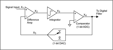
Does SNR improvement only benefit from oversampling and filtering? Note that the 1-bit ADC has an SNR of 7.78dB (6.02 + 1.76). For every 4 increase in the oversampling factor, the SNR is increased by 6 dB, and for every 6 dB increase, it is equivalent to an increase of 1 bit. If the 1-bit ADC is oversampled to 24 times, then a 4-bit resolution is achieved; then an oversampling factor of 415 must be used to achieve 16-bit resolution, which is unrealistic. However, the sigma-delta converter overcomes this limitation with noise shaping techniques, achieving gains of more than 6 dB per 4x oversampling. Noise shapingTo understand noise shaping, we first look at the block diagram of a first-order sigma-delta modulator (Figure 4), which includes a differential amplifier, an integrator, and a comparator, as well as a feedback loop that includes a 1-bit DAC. (The DAC is a simple switch that connects the negative input of the differential amplifier to a positive or negative reference). The purpose of the feedback DAC is to maintain the average output of the integrator close to the reference level of the comparator.
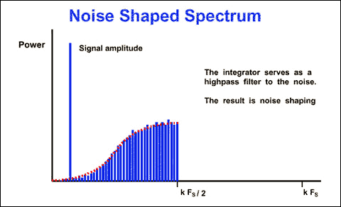
The density of the modulator output "1" is proportional to the input signal. When the input is increased, the comparator generates a large number of "1"; when the input is decreased, the opposite is true. By summing the error voltages, the integrator is a low pass filter for the input signal and a high pass filter for the quantization noise. Therefore, most of the quantization noise is moved to a higher frequency (Figure 5). Oversampling not only changes the total noise power, but also changes its distribution.
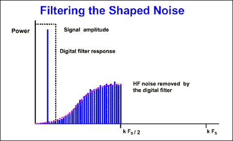
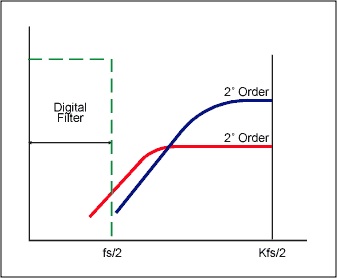
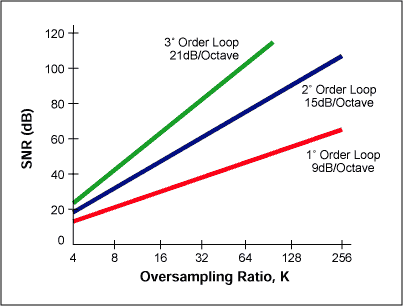
If we add a digital filter to the noise shaping sigma-delta modulator, we can filter out more noise than simple oversampling (Figure 6). This modulator (1st order) provides 9dB SNR improvement for every doubling of the sample rate. For higher order quantization, we can include multiple levels of integration and summation in the sigma-delta modulator. For example, the 2nd order sigma-delta modulator shown in Figure 7 provides a 15dB SNR improvement for every doubling of the sampling rate. Figure 8 shows the relationship between the Σ-Δ modulator order and the oversampling required to achieve a particular SNR.
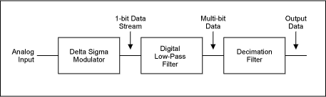
The output of the sigma-delta modulator is a 1-bit data stream with a sampling rate in the megahertz range. The purpose of the digital and sampling filters (Figure 9) is to extract information from the data stream and reduce the data rate to a more useful value. In a sigma-delta ADC, the digital filter averages the 1-bit data stream, increasing the ADC resolution and filtering out-of-band quantization noise. It determines signal bandwidth, settling time, and stopband rejection.
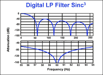
Among the sigma-delta converters, the filter structure widely used to perform the low-pass function is the Sinc3 type (Fig. 10). The main advantage of this filter is its notch response, which can be suppressed, for example, when set to the grid frequency. The notch position is directly related to the output data rate (1/data word period). The setup time of the SINC3 filter is three data word periods. For a 60 Hz notch (60 Hz data rate), the settling time is 3/60 Hz = 50 ms. For applications that require lower resolution and faster settling time, consider the MAX1400 family of ADCs with selectable filter types (SINC1 or SINC3).
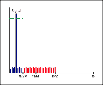
The setup time of the SINC1 filter is a data word. In the above example, 1/60Hz = 16.7ms. Since the digital output filter reduces the bandwidth, the Nyquist criterion is satisfied even if the output data rate is lower than the original sampling rate. To achieve this, specific input samples can be retained while the remaining samples are discarded. This process is referred to as sampling with a factor of M (sampling ratio). If the output data rate is more than twice the signal bandwidth, M can be any integer value (Figure 11). If the input sampling frequency is fs, the filter output data rate can be reduced to fs/M without loss of information.
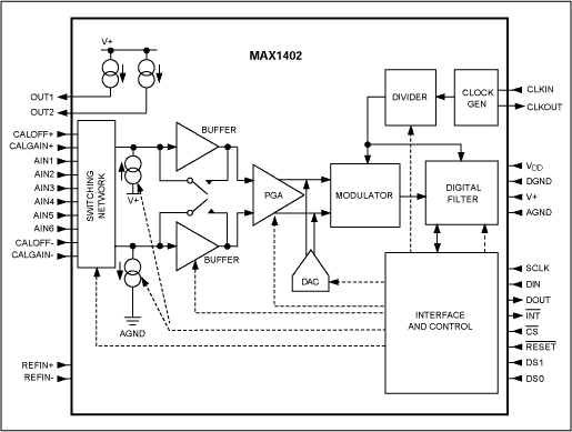
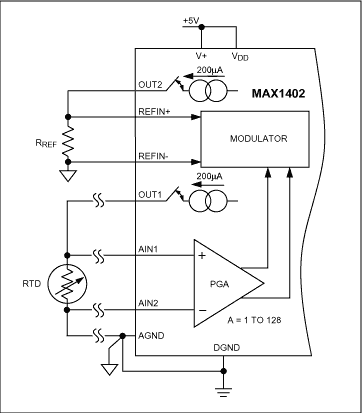
The new highly integrated sigma-delta ADC handles small signals with a minimum number of external components. For example, the MAX1402 chip includes a number of features that are used as on-chip systems (Figure 12). The device's quiescent current is as low as 250μA in active mode (2μA in shutdown mode), 16 bits at 480sps, and 12 bits at 4800sps.
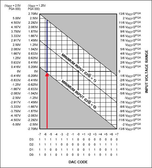
The MAX1402 signal chain includes: a flexible input multiplexer (can be set to three fully differential signals or five pseudo differential signals), two chopper amplifiers, programmable PGA (gain from 1 to 128), for elimination System offset unbalanced DAC, 2nd order sigma-delta modulator. The integrated digital filter can be configured as SINC1 or SINC3 to filter the 1-bit data stream. Conversion results are provided via a SPI/QSPITM compatible, 3-wire serial interface. The chip also includes two fully differential input channels (for calibrating offset and gain), two matched 200μA transmitter excitation currents (for 3-wire and 4-wire RTD applications), and two for testing selected transmitters. A tiny current source for integrity. The device is programmable and accesses eight internal registers through the serial interface to select the operating mode. When the SCAN control bit is set, the enable chip reads the input channel according to the command or continuously; the input channel is represented by a 3-bit "channel identification code" attached to each conversion result. Figure 13 shows the correct input voltage range, determined by the U/B-bar, Vref, PGA, and DAC settings. When the DAC code is "0000", there is no offset. For example, when Vref = 2.5V, set the DAC to "1110", set the PGA to "000", and set the U/B-bar bit to "0" to achieve a full-scale range of 0V to 5V.
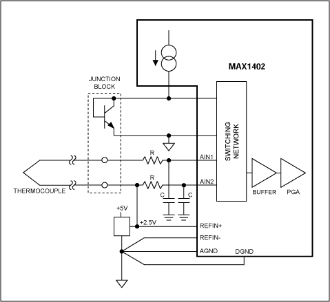
The measurement results can be corrected using two calibration channels (CALOFF and CALGAIN). To achieve this, connect the CALOFF input to ground and the CALGAIN input to the reference voltage. The average measured values ​​of these channels are used in the following interpolation formula: voltage = [Vref & TImes; (code-CALOFF code)] / [(CALGAIN code - CALOFF code) &TImes; PGA gain]. Application of Σ-Δ ADCThermocouple Measurement with Cold Junction Compensation To eliminate the noise picked up by the thermocouple leads, the MAX1402 (Figure 14) in this application uses a buffer mode that allows the front end to have a large decoupling capacitor. In this mode, the AIN2 input must be biased at the reference voltage (2.5V) due to the reduced common mode range. Thermocouple measurements introduce thermoelectric potential problems caused by the connection of thermocouple probes to measuring instruments. This introduces a temperature dependent error that must be subtracted from the temperature measurement to obtain a high precision result.
The voltage measured by the instrument can be expressed as α(T1-Tref), where α is the Seebeck constant of the thermocouple, T1 is the measured temperature, and Tref is the junction temperature. To compensate for the Seebeck coefficient, a portion of the diode-induced temperature compensation voltage (to the thermocouple output) can be added, or the junction temperature can be collected and the compensation value calculated using software. In this mode, the temperature of the pn junction is measured using the differential input channel AIN3-AIN4 and biased by a 200μA internal current generator. High precision thermocouple data acquisition system (DAS)
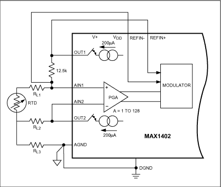
The MAX11200's GPIO controls the precision multiplexer MAX4782, which is either thermocouple or PRTD R1 - PT1000. This method enables dynamic measurement of thermocouples or PRTDs using a single ADC. This design improves system accuracy and reduces calibration requirements. 3-Wire and 4-Wire RTD Configurations Platinum Resistance Temperature Detectors (RTDs) are favored for critical temperature measurements in process control applications due to their excellent accuracy and interchangeability. Platinum PRTD100 produces a 100Ω resistor at 0°C and 200Ω at +266°C. The sensitivity of the RTD is very low (ΔR/ΔT = 100Ω/266°C). When the excitation current is 200μA, 20mV is generated at 0°C and 40mV is generated at +266°C. The analog inputs of the MAX1402 handle these signal levels directly. Errors caused by line resistance can affect measurement accuracy. When the RTD is close to the converter, you can use the traditional 2-wire configuration; but when the RTD is at the far end, the line resistance is superimposed on the RTD impedance, causing a large error. For this type of installation, 3-wire and 4-wire RTD configurations should be used. Two matched 200μA current sources support compensation for errors in 3-wire and 4-wire RTD configurations. In a 3-wire configuration (Figure 16), these current sources pass through RL1 and RL2, ensuring that the AIN1-AIN2 differential voltage is unaffected by line resistance. If the two wires are of the same material and of equal length (RL1 = RL2), the temperature coefficient of the current source is perfectly matched (the MAX1402 temperature coefficient is 5ppm/°C), which is effective.
In the 4-wire configuration, no current is passed through the measurement lines connected to AIN1 and AIN2, so the wireless resistance error (Figure 17). Current source OUT1 provides the excitation current for the RTD, and current source OUT2 provides the current required to generate the reference voltage. The proportional measurement configuration ensures that the reference voltage variation compensates for the RTD temperature coefficient error (caused by the temperature drift of the RTD current source).
High Precision Temperature Data Acquisition System for Platinum Resistance Temperature Detector (PRTD) The MAX11200's DAS provides a very accurate PRTD measurement system that can be used to support RTDs with different resistances over a wide temperature range. Common PRTD resistors are 100Ω (PRTD100), 500Ω (PRTD500), and 1000Ω (PRTD1000). Table 1 shows the differential voltage output ranges for the PRTD100 and PRTD1000 devices. The set of equations on the right calculates the number of noise-free codes for the MAX11200 ADC.
Note that the total range of output signals in a PRTD application is approximately 82 mV. The MAX11200 features extremely low input-referred noise at 570nV at 10sps, making the application's noise-free resolution 0.007°C at 210°C.
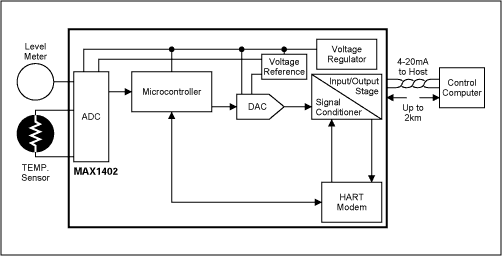
As shown in Figure 18, the GPIO1 pin of the MAX11200 is configured as an output to control the relay calibration switch while selecting a fixed RCAL resistor or PRTD. This versatility improves system accuracy and reduces the calculation of initial values ​​for RA and RT. Smart 4-20mA Transmitter In older 4-20mA transmitters, field-installed devices detect physical parameters such as pressure or temperature and produce a current proportional to the measured variable (standard 4-20 mA range). Advantages of the current loop: The measurement signal is not sensitive to noise and can be powered by the remote. To meet industry requirements, a second-generation 4-20 mA transmitter (called a "smart" transmitter) was developed that uses a microprocessor and data converter to remotely condition the signal. Intelligent devices standardize gain and offset, and linearize sensors such as RTDs and thermocouples: convert to digital signals, process them using mathematical algorithms in μP, convert back to analog signals, and then send standard current through the loop (Figure 19) . The third generation of "smart and smart" 4-20mA transmitters adds digital communication capabilities (to smart devices) that share twisted pairs with 4-20mA signals. This communication channel also allows the transmission of control and diagnostic signals. Low-power devices such as the MAX1402 are suitable because their 250μA supply current saves considerable power for the rest of the transmitter circuitry.
The communication standard of the intelligent transmitter is the HART protocol. The HART protocol is based on the Bell 202 telephony standard and uses the Frequency Shift Keying (FSK) principle. The digital signal includes two frequencies (1200 Hz and 2200 Hz) representing 1 and 0, respectively. To achieve simultaneous analog and digital communication, the sine waves of these frequencies are superimposed onto the DC analog signal cable (Figure 20). Since the average value of the FSK signal is always zero, it does not affect the 4-20 mA analog signal. The response time of the digital communication signal allows approximately 2-3 data updates per second without interrupting the analog signal. The minimum loop impedance required for communication is 23 Ω. 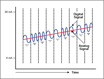 Figure 20. Simultaneous communication of analog and digital. to sum up Prior to the advent of highly integrated conditioning systems, process control was achieved using multiple independent signal conditioning and processing chips. As an alternative, the Σ-Δ solution addresses the performance requirements of the most critical applications while minimizing board space and power requirements (many applications require only 3V or 5V single supplies). Single-supply operation is especially suitable for battery-powered portable systems, where fewer components also increase system reliability. | ||||||||||||||||||||||||||

 for measurement in this paper")
Electric Screw Terminal,Screw Type Terminal Blocks,Screw Type Terminal Blocks Din Rail,Nylon Screw Terminal Block
Wonke Electric CO.,Ltd. , https://www.wkdq-electric.com