Switching power supply products are widely used in LED lighting, instrumentation, air purifiers, security monitoring and other fields. It is a kind of power source that uses modern power electronic technology to control the time ratio of switching tube turn-on and turn-off, and maintain stable output voltage. A pulse width modulation (PWM) control IC and MOSFET are formed.
With the development and innovation of power electronics technology, switching power supply technology is constantly innovating. At present, switching power supplies are widely used in almost all electronic devices due to their small size, light weight and high efficiency. It is an indispensable power supply method for the rapid development of the electronic information industry.
There are two types of modern switching power supplies: one is a DC switching power supply; the other is an AC switching power supply.
The main introduction here is only the DC switching power supply. Its function is to convert the original ecological power (crude power) with poor power quality, such as the mains power supply or the battery power supply, into a high-quality DC voltage that meets the requirements of the equipment. The core of the DC switching power supply is the DC/DC converter.
Therefore, the classification of DC switching power supplies is categorized by DC/DC converters. That is to say, the classification of the DC switching power supply is basically the same as the classification of the DC/DC converter, and the classification of the DC/DC converter is basically the classification of the DC switching power supply.
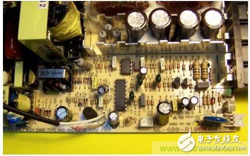
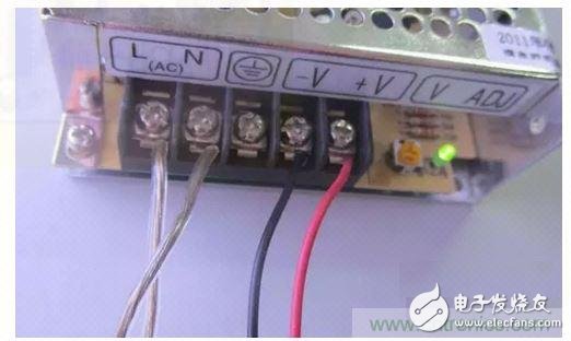
The switching power supply is roughly composed of four main parts: a main circuit, a control circuit, a detection circuit, and an auxiliary power supply.
1, the main circuit
Inrush current limiting: Limits the inrush current on the input side of the power supply.
Input filter: Its function is to filter the clutter in the grid and to prevent the clutter generated by the machine from feeding back to the grid.
Rectification and filtering: directly rectify the grid AC power to a smoother DC.
Inverter: The rectified DC power is changed to high frequency AC, which is the core part of the high frequency switching power supply.
Output rectification and filtering: Provides a stable and reliable DC power supply according to the load requirements.
2, the control circuit
On the one hand, sampling from the output, comparing with the set value, then controlling the inverter, changing its pulse width or pulse frequency to stabilize the output, on the other hand, according to the data provided by the test circuit, the protection circuit provides identification and provides The control circuit performs various protection measures on the power supply.
3, detection circuit
Provides various parameters and various meter data in operation in the protection circuit.
4, auxiliary power supply
Software (remote) startup of the power supply, power supply for protection circuits and control circuits (chips such as PWM).
Here are some classic answers about switching power supplies.
1. Switching power supply transformer If copper strip is used instead of enameled wire, how is the current allowed to pass? For example, a copper strip with a thickness of 0.1mm, how is the current allowed to pass?
â—Experts answer: If the switching power supply transformer replaces the enameled wire with a copper strip, the eddy current loss of the copper strip (enameled wire) can be greatly reduced, and the operating frequency can be increased accordingly, but the DC loss is almost constant, and the current density allowed by the copper strip is generally not required. More than 4.5A/mm2. The current density is equal to the current divided by the cross-sectional area of ​​the conductor, and the cross-sectional area of ​​the conductor is equal to the thickness (0.1 mm) times the width (the width of the copper strip).
2. Is the AC circuit of the AC switch and the rectifier of the power switch the most likely to generate electromagnetic interference?
â—Experts answer: The most serious place for electromagnetic interference generated by switching power supply is the circuit composed of the primary and secondary coils of the switching transformer, but its interference will cause radiation and conduction interference to other circuits through induction, and the most serious conduction and radiation interference. The place is the power line, because the power line is easy to become the half-wave vibrator antenna of the radiation source, and it is connected to the external line, and it is easy to transmit the interference signal to other devices. Therefore, the power supply line must be effectively isolated at the input end of the switching power supply.
3. What is the specific method for reducing the temperature rise of the transformer?
â—Expert answers: One way to reduce the temperature rise of the transformer is to reduce the maximum flux gain (Bm) of the transformer core because of the loss of the transformer core (hysteresis loss and eddy current loss) and the square of the flux density. The ratio is proportional; the other is to reduce the operating frequency of the switching power supply, because the loss of the transformer core (hysteresis loss and eddy current loss) is proportional to the operating frequency; the other is to reduce the loss of the coil, the loss of the coil (mainly eddy current loss) The eddy current loss and the skin effect loss of the coil are also proportional to the operating frequency. To reduce the DC loss of the coil, the current density of the wire must be reduced. Generally, the current density of the enameled wire should not exceed 4.5 A/mm 2 .
4. How does the duty cycle of the flyback switching power supply change?
â— Expert Answer: The duty cycle of the flyback switching power supply is mainly determined by the input voltage and the withstand voltage of the switching power supply tube. When the input voltage changes, the duty cycle also changes. For example, when the input voltage is AC260V, if the withstand voltage of the power switch tube is 650V, the duty ratio is 0.306; when the input voltage is AC170V, the duty ratio is about 0.5; when the input voltage is lower than AC170V, the duty is The ratio is greater than 0.5. But regardless of the input voltage change, the switching power supply will be able to stabilize (or change) the value of the output voltage by changing the duty cycle.
5. What is the difference between positive and negative?
â— Expert Answer: The forward switching power supply is when the power switch is turned on, the power supply is responsible for providing power output, and there is no power output when turned off. The flyback switching power supply is just the opposite. When the power switch is turned on, it only stores energy to the transformer, does not provide power output to the load, and only provides output to the load when the power switch is turned off. The output voltage of the forward switching power supply is the average value of the rectified output voltage. The output voltage of the flyback switching power supply is the half-wave average of the rectified output voltage. The phases of the two voltage outputs are opposite.
6. Can you talk about loop design specifically?
â— Expert answer: The gain of the feedback loop is neither as large as possible, nor as small as possible. When the gain of the feedback loop is too high, the output voltage will track back and forth around the average value. The output voltage fluctuates up and down very much. The higher the gain, the larger the amplitude of the fluctuation. When it is severe, the oscillation occurs. When the feedback loop gains. When it is too low, the output voltage will be unstable again, because the voltage tracking is not in place, there will be a hysteresis error.
In order to stabilize the output voltage without oscillating, the feedback loop is generally divided into three loops. One loop is used to determine the magnitude of the differential gain, the other loop is used to determine the magnitude of the integral gain, and one is Determine the size of the DC gain. The purpose of this is that the loop gain is large when the error signal is small, and the loop gain is smaller when the error is small, that is, the gain of the error amplifier is dynamic. By carefully adjusting the gain of these three feedback loops, the switching power supply can be stabilized without oscillation.
7. How does the flyback power switch MOS get to a minimum? Especially under hard switching conditions.
â— Expert solution: reduce the duty cycle, but the duty cycle is too low, the power supply efficiency is greatly reduced, and the voltage adjustment range is also reduced.
8. What is the ratio of copper foil loss to power loss?
â— Expert answer: very small, if the loss of copper foil is large, the temperature rise of copper foil will be very high, if it exceeds 80 degrees, the paint of copper foil will turn yellow. However, it is only equivalent to the loss of a metal film resistor of about 1 to 3 watts at the same temperature rise.
9. What is the cause of the drive waveform size wave problem? ? I have a power supply. When the low voltage AC85-120V is used, the output drive is normal. When the voltage becomes 120-150V, the drive has a large and small wave, and the output current drops significantly. When the voltage is raised again to 150V-265V, the frequency of the drive waveform is completely out of order, and the output is not correct.
â—Expert answer: If your drive circuit uses capacitor or transformer output, this will happen. Because the capacitor or transformer transmits waveform (signal), the signal can not contain DC component. If it contains DC component, the output waveform will be seriously distorted. Only the output waveform of the driver circuit, when the duty ratio is 0.5, the output waveform will not be distorted, and the duty ratio is too large or too small, and distortion will occur.
10. I would like to ask about the choice of rectifier bridge. What kind of rectifier bridge is used for different power selection? There is also a 30W power supply, using a 3A700V rectifier bridge, found that the rectifier bridge is very hot, not only a few minutes temperature is about 60 degrees. What causes the rectifier bridge to become hot?
â—Expert answers: The choice of rectifier diode is mainly determined by the three parameters of the current flowing through the rectifier diode, the withstand voltage and the operating frequency. When designing the circuit parameters, the current flowing through the rectifier diode can only take the nominal value. One-third (at 25 ° C), because the operating temperature flowing through the rectifier diode may rise above 80 ° C. If the rectifier diode is turned on and off at a very low speed, it will conduct for a period of time in the case of a reverse voltage, that is, the reverse current is very large, so that the rectifier diode will also generate heat. Your rectifier bridge heating may fall into the latter case.
11. How does the feedback loop design and compensation start? I also hope that the teacher will answer the questions patiently.
â— Expert answer: The gain of the feedback loop is neither as large as possible, nor as small as possible. When the gain of the feedback loop is too high, the output voltage will fluctuate around the average value. The higher the gain, the larger the amplitude of the fluctuation. When it is severe, the oscillation will occur. When the gain of the feedback loop is too low, the output voltage will be increased. It will be unstable. In order to stabilize the output voltage without oscillating, the feedback loop is generally divided into three loops. One loop is used to determine the magnitude of the differential gain, the other loop is used to determine the magnitude of the integral gain, and one is Determine the size of the DC gain. By carefully adjusting the gain of these three feedback loops, the switching power supply can be stabilized without oscillation.
12, recently doing DC TO DC efficiency is a bit low, how to solve it?
â—Expert answers: Reduce the working frequency, or replace the power switch tube with a high-speed switch tube. In addition, the volume of the transformer can be increased to reduce the maximum magnetic flux density (Bm), that is, the primary coil of the switch transformer. The number of turns increases because the hysteresis loss and eddy current loss of the switching transformer are proportional to the operating frequency and proportional to the square of the maximum flux density increment.
13. Hello teacher, how do you calculate the minimum DC voltage? I have seen several versions that have not found the most suitable.
â— Experts answer: I don't quite understand what you mean by "minimum DC voltage"? If it is the minimum input DC voltage of the switching power supply, it can generally be converted according to the lowest input AC voltage. For example, if the lowest input AC voltage is AC100V (effective value), the conversion to the lowest DC input voltage is about 120V (average value). Because the maximum value after rectification and filtering is 140V, the lowest value is 100V, and the average value is 120V.
If the minimum DC voltage is the positive feedback voltage of the transistor's self-excited switching power supply, then this voltage is preferably chosen to be twice the operating voltage when the transistor is turned on, and is left as an adjustable margin. If the minimum DC voltage is the minimum operating voltage of the FET driver circuit, the operating voltage must not be less than 16V, because the driving voltage required for deep saturation of the high-power FET is above 12V (preferably 20V).
14. Hello teacher, I have a glitch on the output side of the flyback transformer power supply, and the frequency of the glitch is the same as the primary side switching frequency. How to eliminate the burr?
â— Experts answer: There is a small inductance between the secondary rectification and the filter capacitor, but the inductor cannot be saturated when flowing through the DC. The magnetic loop of this inductor cannot be closed, and a large air gap must be left.
15. Hello teacher! How to optimize the flyback power switching frequency? How is the VOR flyback voltage optimized and under what circumstances is it most appropriate? Thank you! How does Debbie optimize calculations? Thank you.
â—Expert answers: The selection of the operating frequency of the flyback switching power supply is mainly related to the working efficiency and volume of the switching power supply. The working efficiency of the switching power supply is mainly related to the loss of the switching power supply tube and the switching transformer (hysteresis loss and eddy current loss). Relatedly, the losses of both are proportional to the frequency. The loss of the switching power supply tube is mainly composed of the turn-on loss (on-time loss) and the turn-off loss (off-time loss). The longer the on-time and off-time of the switching power supply tube, the larger the two losses.
Generally, the on-time and off-time of the high-power switching power supply tube are much longer than the on-time and off-time of the small-power switching power supply tube, so the operating frequency of the high-power switching power supply is generally lower. When considering the working efficiency of the switching power supply, it is best to consider the volume and cost of the switching power supply.
The selection efficiency is about 80%. At this time, the loss of the switching power supply tube accounts for about 50% of the total loss, and the loss of the switching transformer accounts for about 30% of the total loss. The losses of the remaining circuits account for about the total loss. 20%. The turns ratio of the switching transformer is related to the ratio of the input to output voltage and is related to the duty cycle of the switching power supply.
16, Hello teacher! How to set the initial peak current IP and flyback voltage VOR and the optimized flyback power supply duty cycle, thank you!
â—Expert answers: The magnitude of the flyback voltage generated by the primary and secondary coils of the flyback switching power supply is related to the duty cycle of the switching power supply and to the input voltage. When selecting the duty cycle of the switching power supply, it must be considered. The sum of the flyback voltage peak generated by the primary and the primary coils and the operating voltage (input voltage) cannot exceed 0.7 times the withstand voltage Bvmax of the power switch tube. According to this condition (Bvmax), the flyback switching power supply can be calculated at the highest input voltage. The maximum duty cycle Dmax. For example, Bvmax is a 650V power switch tube. When the input voltage is AC260V, the duty cycle can only be chosen to be around 0.306.
17. Hello teacher! How to optimize the flyback power switching frequency? How is the VOR flyback voltage optimized and under what circumstances is it most appropriate? Thank you! How does Debbie optimize calculations?
â—Expert answers: The selection of the operating frequency of the flyback switching power supply is mainly related to the working efficiency of the switching power supply, and the working efficiency of the switching power supply is mainly related to the loss (hysteresis loss and eddy current loss) of the switching power supply tube and the switching transformer. Both losses are proportional to the frequency. The loss of the switching power supply tube is mainly composed of the turn-on loss (on-time loss) and the turn-off loss (off-time loss). The longer the on-time and off-time of the switching power supply tube, the larger the two losses.
Generally, the on-time and off-time of the high-power switching power supply tube are much longer than the on-time and off-time of the small-power switching power supply tube, so the operating frequency of the high-power switching power supply is generally lower. When considering the working efficiency of the switching power supply, if it is considered from the aspects of the volume and cost of the switching power supply, it is better to select the working efficiency of about 80%. At this time, the loss of the switching power supply tube accounts for about 50% of the total loss. The loss of the switching transformer accounts for about 30% of the total loss, and the losses of the remaining circuits account for about 20% of the total loss. The turns ratio of the switching transformer is related to the ratio of the input to output voltage and is related to the duty cycle of the switching power supply.
18. Hello teacher, I have a glitch on the output side of the flyback transformer power supply, and the frequency of the glitch is the same as the primary side switching frequency. How to eliminate the burr?
â— Experts answer: There is a small inductance between the secondary rectification and the filter capacitor, but the inductor cannot be saturated when flowing through the DC. The magnetic loop of this inductor cannot be closed, and a large air gap must be left.
19. Hello teacher, how do you calculate the minimum DC voltage? I have seen several versions that have not found the most suitable one?
â— Experts answer: I don't quite understand what you mean by "minimum DC voltage"? If it is the minimum input DC voltage of the switching power supply, it can generally be converted according to the lowest input AC voltage. For example, if the lowest input AC voltage is AC100V (effective value), the conversion to the lowest DC input voltage is about 120V (average value). Because the maximum value after rectification and filtering is 140V, the lowest value is 100V, and the average value is 120V.
If the minimum DC voltage is the positive feedback voltage of the transistor's self-excited switching power supply, then this voltage is preferably chosen to be twice the operating voltage when the transistor is turned on, leaving one time as an adjustable margin. If the minimum DC voltage is the minimum operating voltage of the FET driver circuit, the operating voltage must not be less than 16V, because the driving voltage required for deep saturation of the high-power FET is above 12V (preferably 20V).
20, recently doing DC TO DC efficiency is a bit low, how to solve it?
â—Expert answers: Reduce the working frequency, or replace the power switch tube with a high-speed switch tube. In addition, you can increase the volume of the transformer and reduce the maximum magnetic flux density (Bm). The number of turns of the coil increases because the hysteresis loss and eddy current loss of the switching transformer are proportional to the operating frequency and proportional to the square of the maximum flux density increment.
21. Question: How does the feedback loop design and compensation start? I also hope that the teacher will answer the questions patiently.
â— Expert answer: The gain of the feedback loop is neither as large as possible, nor as small as possible. When the gain of the feedback loop is too high, the output voltage will fluctuate around the average value. The higher the gain, the larger the amplitude of the fluctuation. When it is severe, the oscillation will occur. When the gain of the feedback loop is too low, the output voltage will be increased. It will be unstable. In order to stabilize the output voltage without oscillating, the feedback loop is generally divided into three loops. One loop is used to determine the magnitude of the differential gain, the other loop is used to determine the magnitude of the integral gain, and one is Determine the size of the DC gain. By carefully adjusting the gain of these three feedback loops, the switching power supply can be stabilized without oscillation.
KNL4-100 Residual Current Circuit Breaker
KNL4-100 Moulded Case Circuit Breaker is MCCB , How to select good Molded Case Circuit Breaker suppliers? Korlen electric is your first choice. All moulded Case Circuit Breakers pass the CE.CB.SEMKO.SIRIM etc. Certificates.
Moulded Case Circuit Breaker /MCCB can be used to distribute electric power and protect power equipment against overload and short-current, and can change the circuit and start motor infrequently. The application of Moulded Case Circuit Breaker /MCCB is industrial.
Korlen electric also provide Miniature Circuit Breaker /MCB. Residual Current Circuit Breaker /RCCB. RCBO. Led light and so on .
KNL4-100 Molded Case Circuit Breaker,KNL4-100 Small Size Molded Case Circuit Breaker,KNL4-100 Electrical Molded Case Circuit Breaker,KNL4-100 Automatic Molded Case Circuit Breaker
Wenzhou Korlen Electric Appliances Co., Ltd. , https://www.zjmotorstarter.com