Mission-critical servers and communications equipment must be able to operate uninterrupted, even when plugging in and unplugging boards and cards for repair or capacity adjustment. The hot-swap controller IC supports soft-start power supplies to insert or remove boards from a working system, eliminating the need for connection sparks, backplane power supply disturbances, and board resets. The controller IC drives a power MOSFET switch in series with the power supply plugged into the board (Figure 1). After the board is inserted, the MOSFET switch is slowly turned on so that the inrush surge current remains safe when charging the load capacitor.
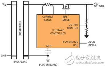
Figure 1: Hot Swap Controller with Pluggable Board
CONNECTORS: Connector
BACKPLANE: Backplane
HOT SWAP CONTROLLER: Hot Swap Controller
When a hot-swap circuit fails, the weak link is typically on the MOSFET switch, which can damage or destroy the hot-swap controller. A common cause of MOSFET failure is the lack of attention to its Safe Operating Area (SOA) at the time of the option. In contrast, when selecting a MOSFET, the drain-source and the maximum drain current (ID(max)) on the resistor (RDS(on)) are mainly considered. Or, the new design is based on an older design with a smaller load capacitance, and the same MOSFET works well. Most power MOSFETs are optimized for low RDS(on) and fast switching. Many power system designers are accustomed to selecting MOSFETs for these characteristics, while MOSFETs transition at significant time in high-loss switching states, but SOA is ignored in the circuit. . There is no SOA in the MOSFET manufacturer's parameter selection table, it does not help. Even with SOA, since the SOA data is usually based on calculations rather than test data, the derating or margin of the application is not obvious.
MOSFET safe working areaSOA is a measure of the power handling capability of a MOSFET during pulsed and DC loads. This is illustrated in the diagram in the MOSFET product manual, as shown in the example in Figure 2. The x-axis is the MOSFET drain-to-source voltage (VDS) and the y-axis is the drain current (ID); both axes use logarithmic coordinates. In this figure, straight lines (each representing a different tP) represent constant MOSFET power. Each line represents the power dissipation allowed by the MOSFET at a pulse width tP, with tP ranging from microseconds to infinity (DC). For example, the figure shows that for a 10ms pulse, there is 5V on the drain-source of the MOSFET, the current flowing through is 50A, and the calculated power consumption is 250W. The lower power dissipation at the same pulse width ensures safe MOSFET operation, labeled as the area below the 10ms line, which is the “safe working areaâ€. Both ends of the figure are determined by the on-resistance, the drain-to-source breakdown voltage, and the maximum pulse drain current.
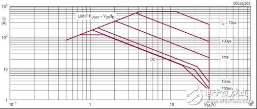
Figure 2: Safe Operating Area of ​​the PSMN3R4-30BLE N-Channel MOSFET
Why is SOA important for hot-swap applications?Most of the power MOSFETs used in the circuit are able to turn on and off quickly, in a high-loss transition state in nanoseconds. In such applications, SOA is not a major issue. In contrast, SOA is very important for hot-swap circuits, providing input inrush current control (soft-start), current limiting, and circuit breaker functions. To understand this, look at the startup waveform of the hot-plugged board (Figure 3a). When the board is plugged into the 12V backplane power supply, the hot-swap controller waits for the connector contact bounce to complete and then soft-starts the MOSFET gate. The output voltage then follows and reaches 12V in 40ms. During this soft start, a 200mA capacitor charge current flows through the MOSFET, and its drain-to-source voltage drops from 12V (= 12VIN − 0VOUT) to almost 0V (= 12VIN − 12VOUT). When a short circuit occurs on the load (Figure 3b), the controller limits the current on the MOSFET to 6A and the voltage is 12V (= 12VIN − 0VOUT). This 72W power state lasts for 1.2ms until the circuit breaker timer expires. In the case of starting surges and current limiting, hot-swap MOSFETs are required to handle significant power consumption for hundreds of microseconds to tens of milliseconds, and attention should be paid to their SOA performance.
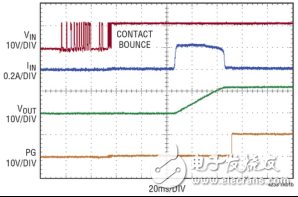
Figure 3a. Soft Start When the Board Is Hot Plugged into the 12V Backplane Power Supply
CONTACT BOUNCE: Contact rebound
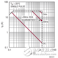
Figure 3b. Current limit during output short circuit
CONTACT BOUNCE: Contact rebound
SINGLE PULSE: Single pulse
GUARANTEED: Guaranteed
Integrated MOSFET hot-swap controller with guaranteed SOALinear Technology offers a family of hot-swap controllers with integrated MOSFETs that simplify the hot-swap designer's work by eliminating the need to spend time searching for MOSFET data for optimal fit. The latest models in this series, the LTC4233 and LTC4234 (Figure 4), are 10A and 20A hot-swap controllers with integrated MOSFET and current sensing. They range from 2.9V to 15V and cover standard 3.3V, 5V and 12V power supplies. . By integrating the two most critical and largest hot-swappable components (power MOSFETs and sense resistors), these controllers help reduce design time and board space, adding more valuable features to the final product.
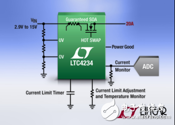
Figure 4: LTC4234: 20A Guaranteed SOA Hot Swap Controller
Guaranteed SOA: Guaranteed SOA
HOT SWAP: Hot swap
Power Good: Power is good
Current Monitor: Current Monitor
Current Limit TImer: Current Limit Timer
Current Limit Adjustment and Temperature Monitor: Current Limit Adjustment and Temperature Monitor
A unique feature of the LTC4233 and LTC4234 controllers is that their internal MOSFET SOA is guaranteed in the product manual, which is not found in stand-alone MOSFETs. The SOA per device is tested for production at a single point in the SOA diagram. Figure 5 shows the SOA plot of the LTC4234. Applying 13.5V from the input to the output, the output source is 6A for 30ms to test its SOA. The resulting power consumption is 81W. This is indicated by a red dot in the SOA diagram. The LTC4233 was tested with the same voltage, except that the current and power were halved (ie 3A and 40.5W for 30ms). Note that the LTC4233 and LTC4234 SOA plots show a guaranteed minimum SOA, while the MOSFET datasheet shows typical values.

Figure 5: LTC4234 Hot Swap Controller Guaranteed Safe Work Area Diagram
SINGLE PULSE: Single pulse
GUARANTEED: Guaranteed
The LTC4233 and LTC4234 also output a ground reference signal that is proportional to the load current through the internal sense resistor. An external analog-to-digital converter (Figure 4) can be used to measure this output, providing system administrators with board current and power consumption data. The current limit is reduced from its default value by an external resistor so that it can be quickly adjusted to accommodate dynamic load changes and various applications. Optional undervoltage and overvoltage thresholds protect the downstream load from exceeding the effective window voltage, preventing circuit failure and damage. The controller can be used to implement inrush current control, current limit, and circuit breaker functions even where hot insertion is not required. Typical applications for these controllers include space-constrained high-density boards and cards in mission-critical servers, network routers and switches, enterprise SSD storage, and industrial systems.
in conclusionIn addition to the hot-swap controller itself, the hot-swap circuitry protects the board power and MOSFET failures from damaging the expensive processing electronics downstream of the MOSFET. Field failures, exposure to MOSFET weaknesses, etc. can result in high recycling and damage to reputation. Therefore, it is important to ensure that the MOSFET is selected to reliably handle the stresses encountered in hot-swap applications. The LTC4233 and LTC4234 integrate MOSFET hot-swap controllers, reducing solution footprint, design time, and new product testing for each controller SOA, ensuring a rugged and reliable solution.
Thin film transistor liquid crystal display, commonly referred to as the TFT-LCD, is a type of liquid crystal display that USES thin-film transistor technology to improve the image quality. Although TFT-LCD is collectively known as LCD, it is an active matrix LCD used in televisions, flat screens and projectors.
Simply put, the TFT-LCD Panel can be seen as a layer of liquid crystal sandwiched between two glass substrates, the upper glass substrates being color filters, and the lower glass having transistors embedded in it. When the current passes through the transistor, the electric field changes and the liquid crystal molecules deflect, so as to change the polarization of the light, and then the polarizer is used to determine the light and dark state of the pixel. In addition, the upper glass is fitted to the color filter, so that each pixel contains three colors of red, blue and green, which make up the video image on the panel.
The Thin film Liquid Crystal Display is a type of most liquid crystal display that USES thin-film transistor technology to improve the image quality. Although TFT-LCD is generally referred to as LCD, it is an active matrix LCD. It is used in TV, flat panel display and projector.
I2C Tft Display,4.3 Inch Display,Lcd 4.3 Inch,Arduino 3.5 Tft Lcd
Tonya Display Limited , https://www.tydisplay.com