An analog to digital converter (A/D converter, or ADC) is usually used to convert an analog signal into a digital signal. As an important component in the analog circuit, this article will introduce the basics of the principle, classification and technical indicators of the analog-to-digital converter.
ADC developmentWith the rapid development of electronic technology and the widespread use of computers in automatic detection and automatic control systems, the use of digital systems to process analog signals has become more common. Digital electronic computers process and transmit discontinuous digital signals, but most of the actual encounters are continuously varying analog quantities. After the analog quantity is converted into the analog quantity of the electrical signal by the sensor, it needs to be converted by analog/digital conversion. The digital signal can be input into the digital system for processing and control, and thus serves as an interface circuit for converting analog power into digital output. The A/D converter is a bridge between analog signals and digital signals in the real world, and is an electronic technology development. The key and the bottle are located.
Since the introduction of the A/D converter, it has experienced the development of discrete semiconductors and integrated circuit data converters. In the integration technology, modular, hybrid and microcontroller integrated data converter technology has been developed. In this process, process technology has been greatly improved. The monolithic integrated circuit process technology mainly includes a bipolar process, a CMOS process, and a BiCMOS process combining bipolar and CMOS. Modules, hybrids, and monolithic integrated converters have evolved to leverage each other's strengths and complement each other, developing A/D and D/A converters for different application requirements. In recent years, there have been thousands of converter products.
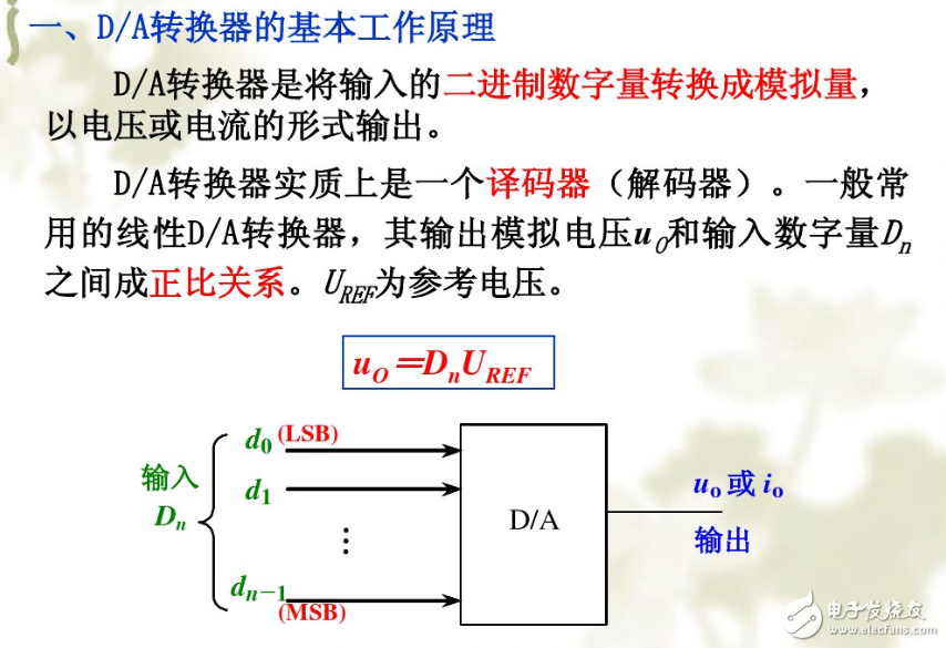
ADC principleThe D/A converter converts the input binary digital quantity into an analog quantity and outputs it in the form of voltage or current.
Analog-to-digital conversion generally involves several steps of sampling, holding, and quantifying and encoding.
The main type of ADCThere are many types of ADCs, such as traditional parallel, successive approximation, and integral ADCs. There are also new ∑-Δ and pipeline ADCs that have been developed in recent years. Many types of ADCs have their own advantages and disadvantages and can meet Different specific application requirements. Low power consumption, high speed and high resolution are the development direction of the new ADC, and this development direction of ADC will adapt to the development of modern digital electronic technology.
Parallel comparison ADC
Parallel comparison ADCs are today's fastest analog-to-digital converters with sampling rates above 1 GSPS and are often referred to as "flashing" ADCs. It consists of a resistor divider, a comparator, a buffer, and an encoder. The conversion of all bits of the ADC of this structure is completed at the same time, and the conversion time mainly depends on the switching speed of the comparator, the transmission time delay of the encoder, and the like. Increasing the output code has less impact on conversion time, but as resolution increases, a high-density analog design is required to achieve the large number of precision divider resistors and comparator circuits necessary for conversion. The output number is increased by one, the number of precision resistors is doubled, and the comparator is approximately doubled.
The resolution of a flash ADC is limited by the die size, excessive input capacitance, power consumption of a large number of comparators, and so on. As a result, repeated parallel comparators can cause static errors if the accuracy does not match, such as increasing the input offset voltage. Similarly, this type of ADC also produces discrete, inaccurate outputs due to the sub-regulation of the comparator, encoding bubbles, the so-called "spark code." The advantage of this type of ADC is that the analog/digital conversion speed is the highest, and the disadvantage is that the resolution is not high, the power consumption is large, and the cost is high.
The modern development of high-speed ADC circuit structures mainly uses this fully parallel ADC, but due to power and volume limitations, it is unrealistic to manufacture high-resolution flash ADCs.
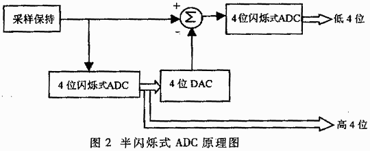
A higher resolution semi-flash ADC or stepped ADC consisting of two lower resolution scintillation ADCs is the primary means of manufacturing high speed ADCs in the world today. Figure 2 shows the block diagram of an 8-bit two-stage parallel half-sparkling ADC. The conversion process is divided into two steps:
The first step is coarsening and quantification. The high-order 4-bit conversion is first performed in parallel, and the converted high-order 4-bit output is simultaneously converted to an analog voltage by D/A conversion of the digital output.
The second step is to further refine the quantification. The original input voltage is subtracted from the analog voltage output from the D/A converter, and the difference is further reduced by 4 full A/D conversion. The digital outputs of the two-stage A/D converter described above are then connected in parallel as a total output. In this way, a little sacrifice is made in the conversion speed, but the contradiction between the resolution improvement and the increase in the number of components is solved.
Successive approximation ADC
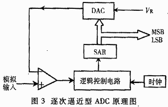
The successive approximation ADC is a widely used analog-to-digital conversion method. It consists of a comparator, a D/A converter, a comparison register SAR, a clock generator, and a control logic circuit. The sampled input signal is continuously compared with a known voltage. And then converted to a binary number.
The schematic diagram is shown in Figure 3. First, the most significant bit MSB of the DAC is saved to the SAR, and then the voltage corresponding to the value is compared with the input voltage. The comparator output is fed back to the DAC and corrected before a comparison. Under the logic control circuit and clock drive, the SAR continuously compares and shifts until the LSB transition is completed. The resulting DAC output approaches ±1/2LSB of the input voltage. When each bit is determined, the conversion result is latched into the SAR and output as an ADC.
Integral ADC
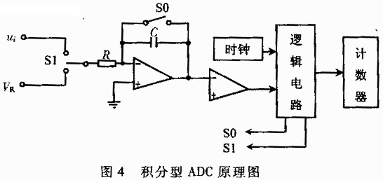
Integral ADCs, also known as dual-slope or multi-slope ADCs, are a widely used class of converters. Its basic principle is to convert the input analog voltage into a time interval proportional to its average value by two integrations. At the same time, the clock is counted by the counter during this time interval, thereby realizing A/D conversion. The schematic diagram is shown in Figure 4. Its work is divided into two phases, the first phase is the sampling period and the second phase is the comparison period. The digital value D = 2nV1/VR of the analog signal can be obtained by counting the two integrals and the counter, where n is the number of bits of the counter and V1 is the average value of the input voltage over a fixed time interval.
Voltage-to-Frequency ADC
The parallel comparison ADC and the successive approximation ADC mentioned above are all direct conversion ADCs, while the integral type and the voltage conversion ADC described below are indirect ADCs. The voltage-frequency conversion ADC first converts the voltage of the input analog signal into a pulse signal whose frequency is proportional to it, and then counts the pulse signal at a fixed time interval, and the counting result is a digital quantity proportional to the input analog voltage signal. . In theory, the resolution of such an ADC can be increased indefinitely, as long as the length of the cumulative number of pulses required to meet the output frequency resolution is used. The advantages are: high precision, low price and low power consumption. The disadvantage is that similar to the integral ADC, the conversion rate is limited, from 100 to 300 SPS at 12 bits.
All our items Suitable for space like meeting room, living room as well as restaurant, leisure club,office etc;
And all are packed in singel neautral box safely, mass production in carton case approved by drop test. We can make custom logo and box for bulk cargos. Please click to contact us freely if you have the query. We have different shipping options for you: Express, Air, Sea. Please choose your favorite way, or you can also refers to our recommendation.
We have our own Control systems: Shorten lead times at low cost with responsive production planning and with many years experience of producing products.
We could provide OEM / ODM service for all kinds of customers. Our professional support team will service online 24 hours for customers.
We have a very strong quality control Samples are always available for checking quality and Efficient Logistics.
Professional Design Team: artwork/ Instruction manual/ product design according to customer's requirements.
Wifi Diffuser,Smart Humidifier,Smart Oil Diffuser,Electric Aromatherapy Diffuser
KIWA ELECTRONIC (HK) INDUSTRIES CO.,LTD , https://www.kiwahk.com