design background:
The ROM is an abbreviation of read-only memory, and is a solid-state semiconductor memory that can only read data stored in advance. Its characteristic is that once the data is stored, it cannot be changed or deleted. It is usually used in electronic or computer systems that do not require constant data changes, and the data does not disappear because the power is turned off.
ROM is composed of the first letter of English Read only Memory, which means read-only memory. As the name implies, such a memory can only be read, and cannot be read and written at any time like RAM. It only allows the opportunity to write once after it is produced. Data cannot be changed once it is written. Another characteristic of it is that the data inside the memory is not lost after being powered off, and can be stored for hundreds of years. This kind of memory is mostly used to store firmware, such as computer-initiated boot programs, mobile phones, MP3, MP4, digital cameras and other electronic products corresponding to the program code.
Design principle:
Our design reads the data from the ROM, reads the last data, and then reads the data back from the last address to achieve a cyclical reading.
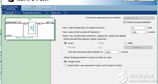
First of all, we first create a .mif file, and then write the corresponding address, such as data, and then design an IP core, and then read the ROM address, read out the data in the ROM, the specific operation as follows.
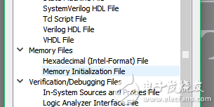
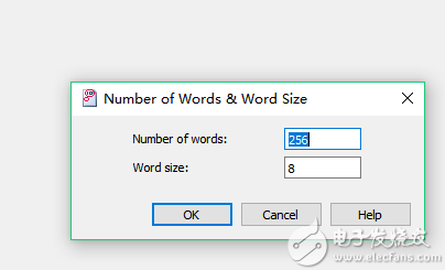
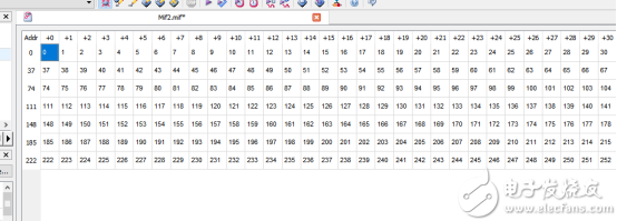
Next, create a .mif with a depth of 256 and a bit width of 8.
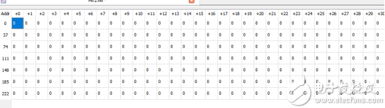
Then right click on the first address.
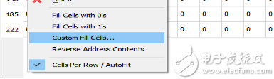
Fill in the start address and the end address. We write the same data as the address for each address bit. Then the data starts from 0, steps to 1, as follows, and then completes and saves.

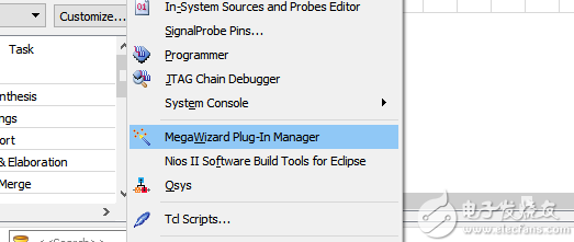
So we write our .mif file and then follow the steps below.
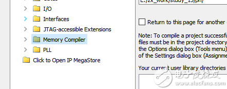
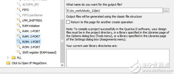

Select our hardware description language of choice, we are all verilog HDL, and then select the path we generated the file, the next step.
Set the bit width and depth of our output, our depth 256, bit width 8, and the next step.
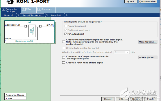
Remove the output check whether the register, if you select the output will be a beat later, because of the addition of an output register.
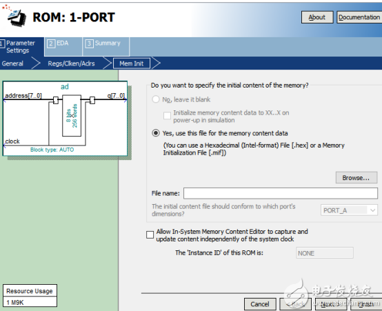
Then the following interface appears, click  , Select the .mif file we generated, add it, then go to the next step and complete the next step.
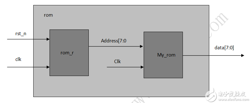
Design architecture diagram:
Design code:
Top level module
0 module rom(clk,rst_n,data);
1 input clk;
2 input rst_n;
3
4 output [7:0] data;
5
6 wire [7:0]address;
7
8 rom_r rom_r ( // Instantiation ROM controller module
9 .clk(clk),
10 .rst_n(rst_n),
11 .address(address)
12);
13
14 my_rom my_rom_inst ( // Instantiation IP core module
15 .address ( address ),
16 .clock ( clk ),
17 .q (data )
18);
19
20 endmodule
Design module
0 module rom_r(clk,rst_n,address);
1
2 input clk;
3 input rst_n;
4
5 output reg [7:0] address;
6
7 reg [1:0] state;
8 always @(posedge clk or negedge rst_n)
9 if(!rst_n)
10 begin
11 address <= 1'b0;
12 state <= 1'b0;
13 end
14 else
15 begin
16 case (state)
17 0:begin
18 if (address < 255) // determine the address
19 begin
20 address <= address + 1'b1; // address increase
21 end
22 else
23 begin
24 if(address == 255) //Deciding whether to finish reading
25 begin
26 address <= address - 1'b1;
27 state <= 1;
28 end
29
30 end
31 end
32 1:begin
33 if(address > 0) // After reading a state jump to make the address minus 1
34 begin
35 address <= address - 1'b1;
36 end
37 else
38 begin
39 address <= address + 1'b1;
40 state <= 0;
41 end
42 end
43 default : state <= 0;
44 endcase
45 end
46 endmodule
Test module
0 `timescale 1ns/1ps
1
2 module rom_tb();
3
4 reg clk;
5 reg rst_n;
6
7 wire [7:0] data;
8
9 initial begin
10 clk = 1'b1;
11 rst_n = 1'b0;
12
13 #100.1 rst_n = 1'b1;
14
15 #20000 $stop; // Stop simulation after 20000NS
16
17 end
18
19 always #10 clk = ~clk; //Generate 50M clock
20
21 rom rom_dut ( // instantiate the top level module
22 .clk(clk),
23 .rst_n(rst_n),
24 .data(data)
25);
26 endmodule
Simulation diagram:
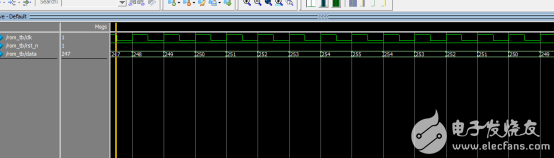
In the simulation we can see that as with our design, we first read data from address 0, read the last number, and then return to read from the last address.
Tws Sport Earphone,True Wireless Earbuds,Tws True Wireless Stereo,Tws True Wireless Earbuds
Guangzhou YISON Electron Technology Co., Limited , https://www.yisonearphone.com