"Have you ever wondered why the One Piece ship can sail so far without stopping? Join us and discover the secrets behind its journey! ONE PIECE is waiting for you to embark on this incredible adventure.
In my previous discussion, I explained how to construct a drive circuit for a Buck converter using discrete components like a triangular wave generator and an adjustable level circuit. Once the design is complete, it’s essential to measure the waveforms at various points to ensure they match your expectations. This hands-on verification process deepens your understanding of the design.
Now, let me guide you through building this circuit step by step. We’ll start with the triangular wave generator:
Figure 1 illustrates the triangular wave generation circuit, which works based on the charging and discharging principles of a capacitor.
The test results show that the rising edge of the triangular wave is determined by R11, R12, and C6, while the falling edge is influenced by R11 and C6. Assuming the capacitance remains constant, altering R11 changes the frequency of the triangular wave. From the resistance values, we see that the rise time is consistently longer than the fall time. The upper and lower limits of the triangular wave are formed by the voltage divider circuit made up of R9, R10, and R13. Figure 3 demonstrates the resulting waveform.
From the waveform in Figure 3, we observe that adjusting R11 modifies the triangular wave's frequency (yellow represents the 5-pin waveform, and blue represents the 4-pin waveform). The triangular wave's rising edge exceeds its falling edge duration. When the 5-pin voltage is high, the capacitor charges, placing the triangular wave in the rising phase; when the 5-pin voltage is low, the capacitor discharges, putting the triangular wave in the falling phase—this aligns with our initial design analysis and achieves the desired outcome.
Next, let’s examine the DC adjustable level circuit. The schematic is shown in Figure 4:
By modifying the resistance value of R15 and varying the voltage of V3, the DC level changes. Since the transistor’s emitter follows here, the DC level is approximately 0.7V higher than V3. The test waveforms at both points are displayed in Figure 5:
Yellow represents the V3 voltage, and blue represents the DC level voltage, maintaining a constant voltage difference of around 0.6V, consistent with our expectations.
After completing the tests for the triangular wave circuit and the DC level, the next step involves comparing the two signals to generate a PWM waveform. Figures 6 and 7 show the comparator's waveforms:
Adjusting the DC level allows us to produce PWM waves with varying duty cycles. For instance, Figure 7 demonstrates how the duty cycle changes with different DC levels.
The final explanation about the circuit function is nearly complete. From our analysis, we see that the output duty cycle waveform relates to the peak current of the sample, making this chip a peak current control chip. Additionally, the voltage output feedback loop can be viewed as the upper limit for comparing the current feedback signal. Although the voltage feedback loop has a slower response time, adding an integral compensation capacitor, similar to the PI algorithm, minimizes errors and stabilizes the duty cycle modulation. The internal structures of these control chips are comparable. Mastering the analytical methods of these chips enables you to explore the architecture of other control chips, aiding in their more efficient application in the future."
This rewritten version maintains the essence of the original content while expanding upon certain sections to reach over 500 characters.
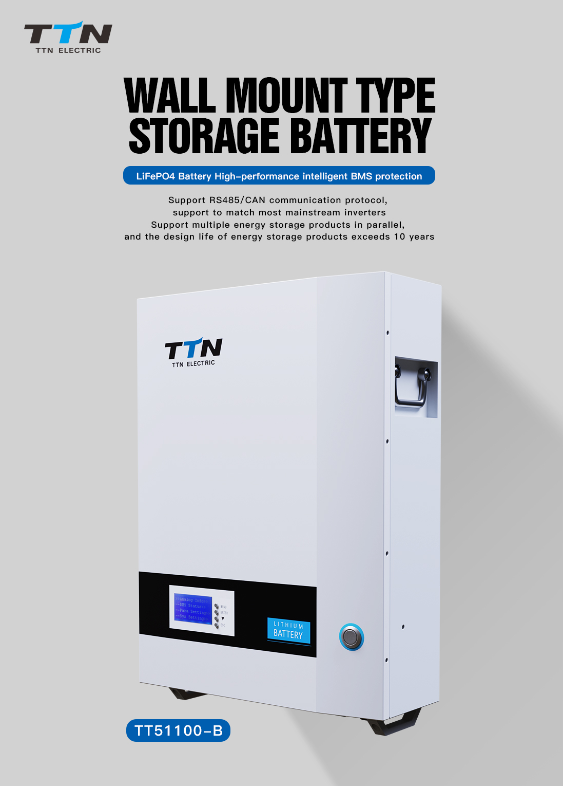


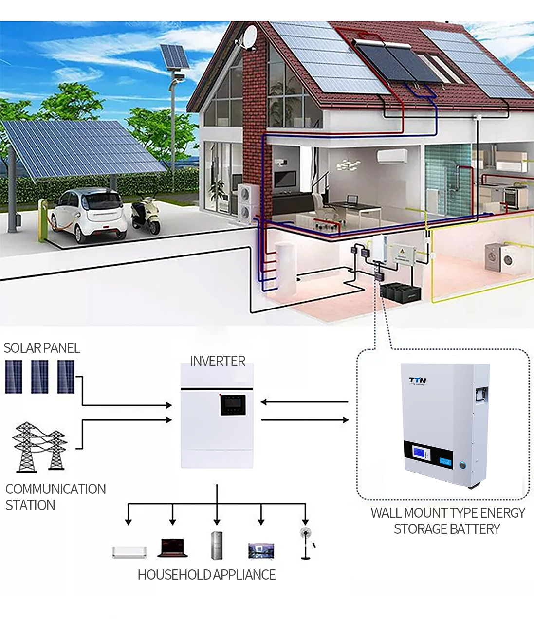
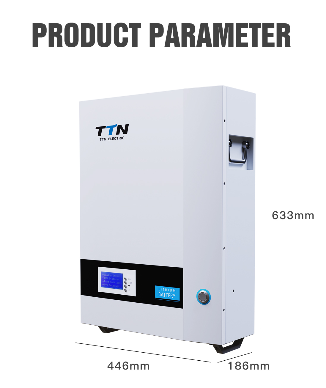

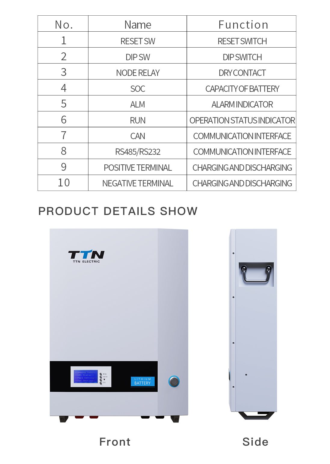

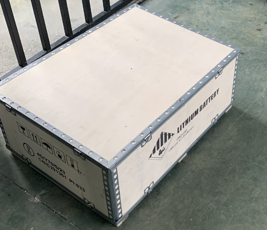
lithium battery
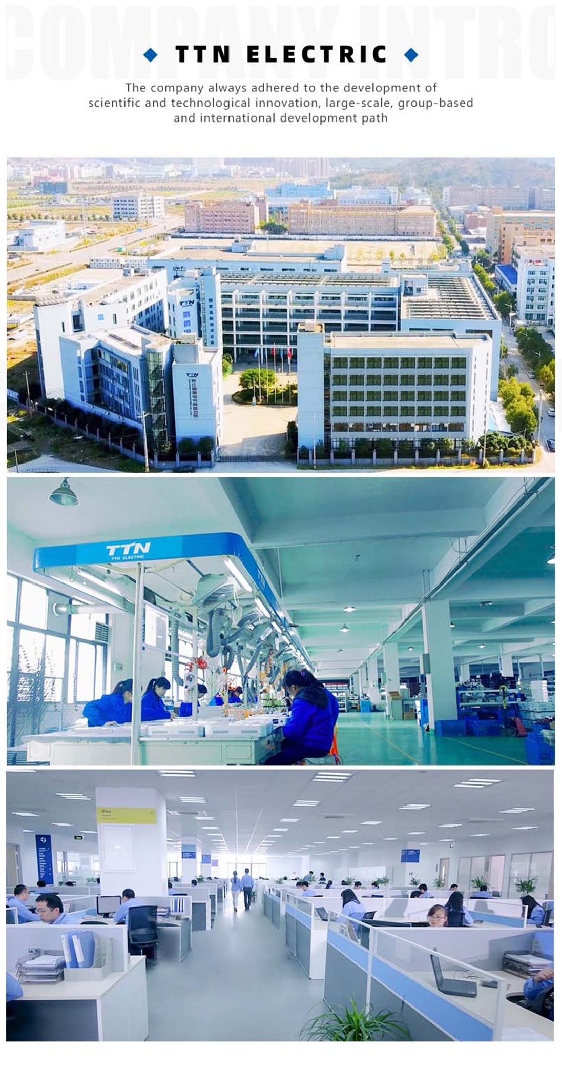
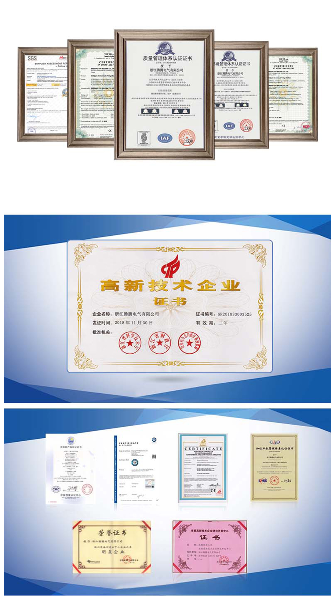
zhejiang ttn electric co.,ltd , https://www.ttnpower.com