China's LED industry has begun to take shape. From the perspective of LED main technical indicators, there is still a lot of room for promotion. It is necessary to increase the research and development of LED, master the core technology of LED, break through the foreign patent restrictions, and further expand the semiconductor at home and abroad. The lighting market will expand the scale of China's LED industry and provide people with energy-saving, environmentally friendly, healthy and comfortable lighting environment. The overview of the chip field is as follows (not counted in 2015) and is for reference only.
LED substrate profile
The substrates currently used for LED industrialization are mainly sapphire (Al2O3), SiC, Si and GaN.
CREE uses SiC substrate, many companies around the world are developing Si substrate, Toshiba has announced the production of 8′′ Si substrate. The rest of the company is mainly sapphire, with more than 130 sapphire substrates produced worldwide, of which more than 80 are nearly two. It was added in the year. It is mainly based on 2′′ and 4′′ substrate sheets. After a few years, it will be 6′′, which will reach more than 50%. It is predicted that in 2016, three types of substrates, sapphire, Si and GaN, will each account for one-third. In recent years, many new LED substrates have been researched and developed around the world, and breakthroughs have been made.
China has developed and produced more than 50 sapphire substrates, of which more than 20 have been put into production. China's production capacity has exceeded 100 million pieces per year (calculated in 2′′), exceeding global demand, and sapphire companies directly produce PSS linings. There are not many bottoms. At present, sapphire is about 50% localized, and the competitiveness of enterprises is poor. It is inevitable to go to transformation, integration and merger. In addition, Nanchang Jing can use Si substrate to mass produce LEDs. There are many research institutes in China. The company is developing homogenous substrates, composite substrates and SiC substrates, and has achieved great results.
LED epitaxy and chip industry profile
There are about 169 LED epitaxial and chip R&D production units in the world (another reported 142), and there are about 3,000 MOCVD equipment (also reported as 2,800 units), and its production capacity is 4 million pieces per month. The proportion is about 25.8% in China, 21.8% in Taiwan, 19.2% in Japan, 17.3% in South Korea, 11% in the US, and 2.8% in Europe.
There are more than 50 LED epitaxial and chip companies in China, among which more than 30 are put into production, the operating rate is 50~60%, the output exceeds 100 billion (including small chip and quaternary chip), and the output value is about 8.4 billion yuan (other reports) It is 10.5 billion yuan). Due to the excessive number of upstream enterprises in China, most enterprises are small in scale, and integration and merger are inevitable. In addition, there are dozens of companies in China that are developing and manufacturing MOCVD equipment, and some have already been tested or officially put into production in upstream enterprises. There are also MO sources for epitaxy: trimethyl (gallium, indium, aluminum, antimony), triethyl (gallium, antimony), dimethyl zinc, diethyl (zinc, antimony) and other localization rates have reached 60 %.
LED main technical indicators
The laboratory level of several large companies such as Nichia, Philips, and Oslo has a luminous efficacy of more than 200 lm/w, and Cree's laboratory efficacy has exceeded 276 lm/w. Seoul Semiconductor "npolo" LED, claiming to achieve 1000 luminous flux on a 1mm2 chip, Mitsubishi Chemical also proposed a luminous flux of 1000lm, called the ultimate goal of LED light source. Japan's Tamura production proposed to achieve 2000~3000 lm luminous flux in 2mm square chips. The University of California, Santa Barbara, proposed a luminous efficacy of 300 lm/w. The US company Soraa uses GaN-on-GaN technology to make LED replacement lamps, so that each lamp uses a LED device to write a new chapter in LED technology, namely LED version 2.0. In the US SSL plan revision, the LED light effect industrialization level reached 266 lm/w as the ultimate goal. At present, the global LED industrialization light efficiency level is 120~150 lm/w.
Luminous new material
In the future, new luminescent materials may enter the field of lighting and compete with LED lighting.
(1) Organic light emitting diode
At present, the effective light effect of OLED is generally 30~60 lm/w, which will be applied in the field of special lighting. According to foreign institutions, the OLED lighting market will reach more than 40 billion U.S. dollars in 2021, and another agency is expected to reach 40 billion U.S. dollars in 2018. The main problems at this stage are high prices, except for certain technologies, but the outlook is optimistic.
(2) Quantum dot luminescence technology
Quantum dots (Quantun Dot abbreviated QD) are fabricated by nanotechnology. QD particles are generally between 2 and 12 nm. Quantum dot illuminants consist of luminescent nuclei, semiconductor shells, and organic ligands, excited by electric or short-wave light. It emits light of different wavelengths, close to the continuous visible light spectrum. For example, CdSe (cadmium selenide) emits blue light when the particle is 2.1 nm, emits green light when it is 5 nm, and emits near red light when it is close to 10 nm. Its advantages are: stable light emission, internal quantum efficient.
At present, the quantum dot luminous efficiency is close to the OLED level. QD illumination has a wide range of applications. In addition to display and illumination, it can also be applied to blue laser, light sensing components, single-electron transistors, memory storage... At this stage, QD is mainly displayed. A significant effect on the application will be the most promising alternative to OLED. In combination with LEDs in lighting, it produces a rich, bright, warm white light.
(3) Ultra-thin amorphous dielectric layer light-emitting chip
A light-emitting chip developed by the Department of Chemical Engineering of Texas A&M University in the United States, using a room temperature sputtering deposition method on a silicon crystal garden to form a dielectric film, in which a nanocrystalline layer can enhance the light-emitting density, and can be used in the process. Silicon IC compatible, simple process, is a new nano luminescent material technology. Although the current luminescence lifetime is shorter, it will be longer in the future.
Summary: The above-mentioned several new luminescent materials, the share of OLED in the field of lighting will increase sooner and later, and will occupy a certain proportion in the special lighting field. As for the quantum dots and the light-emitting layers in the ultra-thin medium are nano-scale quantum layers, which are new materials for nano-luminescence. It is necessary to attach great importance to the research and development of nano-luminescence technology, and it is possible to enter the field of illumination in the future and replace LED lighting products.
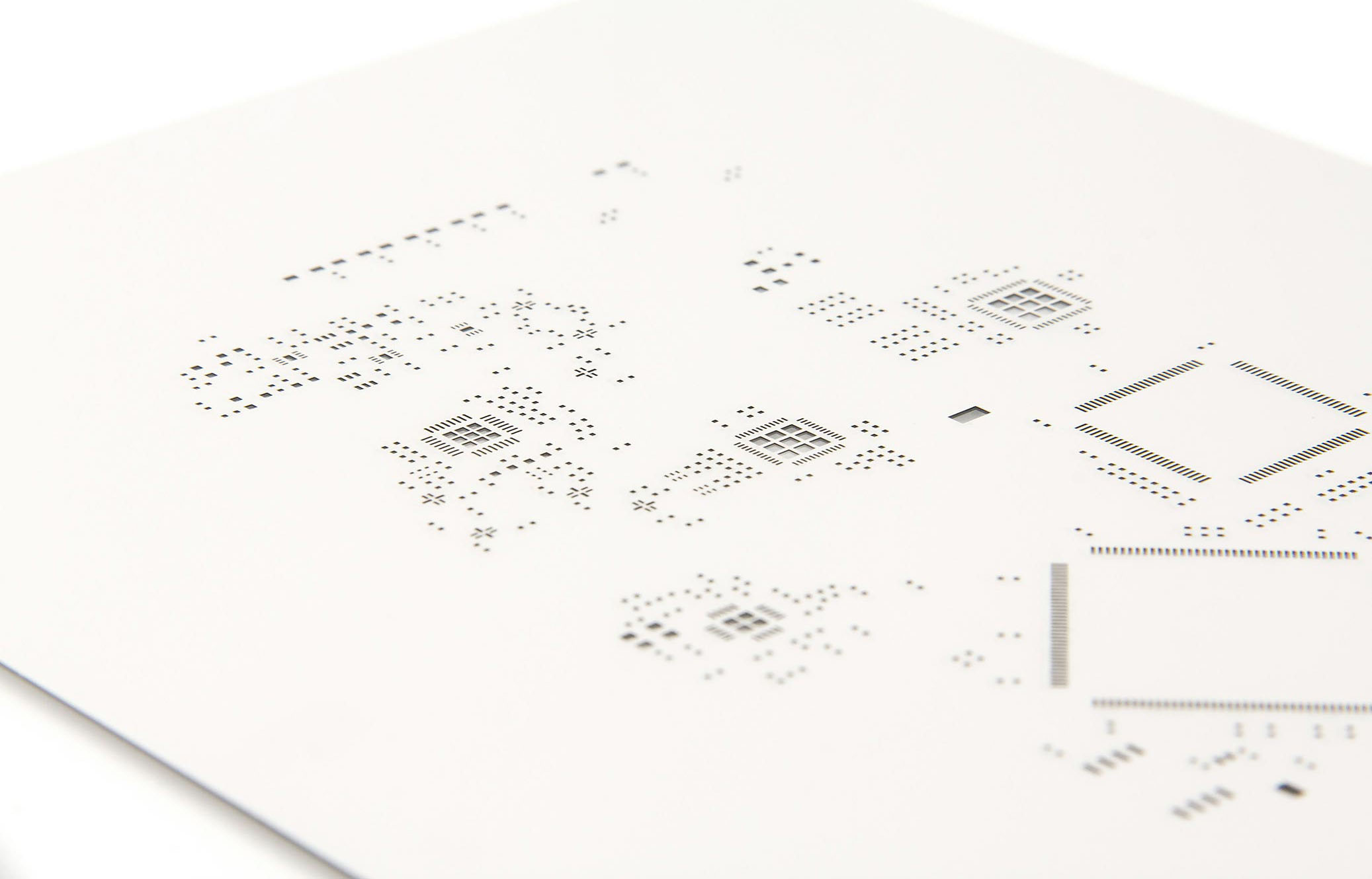
PCB SMT Stencil ,the unique goal is to move solder paste to the bare Printed Circuit Board.
PCB Stencil , SMT Stencil, SMD Stencil , Laser Stencil , What is it?
Apart from all types of Printed Circuit Boards (PCBs) such as Prototype PCB , Aluminum PCB , HDI PCB , Flexible PCB , Rigid Flex PCB , Thick Copper PCB, High TG PCB , JHYPCB also manufactures solder paste stencils to meet Surface Mount Technology (SMT) requirements.
PCB Stencils, also called SMT stencils, SMD stencil, play a key role in transferring accurate amount of solder paste to correct positions on bare circuit boards ready for assembly. In other words, stencils can fast and efficiently ensure the most accurate solder paste amount and optimal electrical connection. With solder stencils, it is possible to use metal squeegee blades to apply solder paste easily over the openings on PCBs and make stencil to be well aligned with the surface of the advanced circuit board.
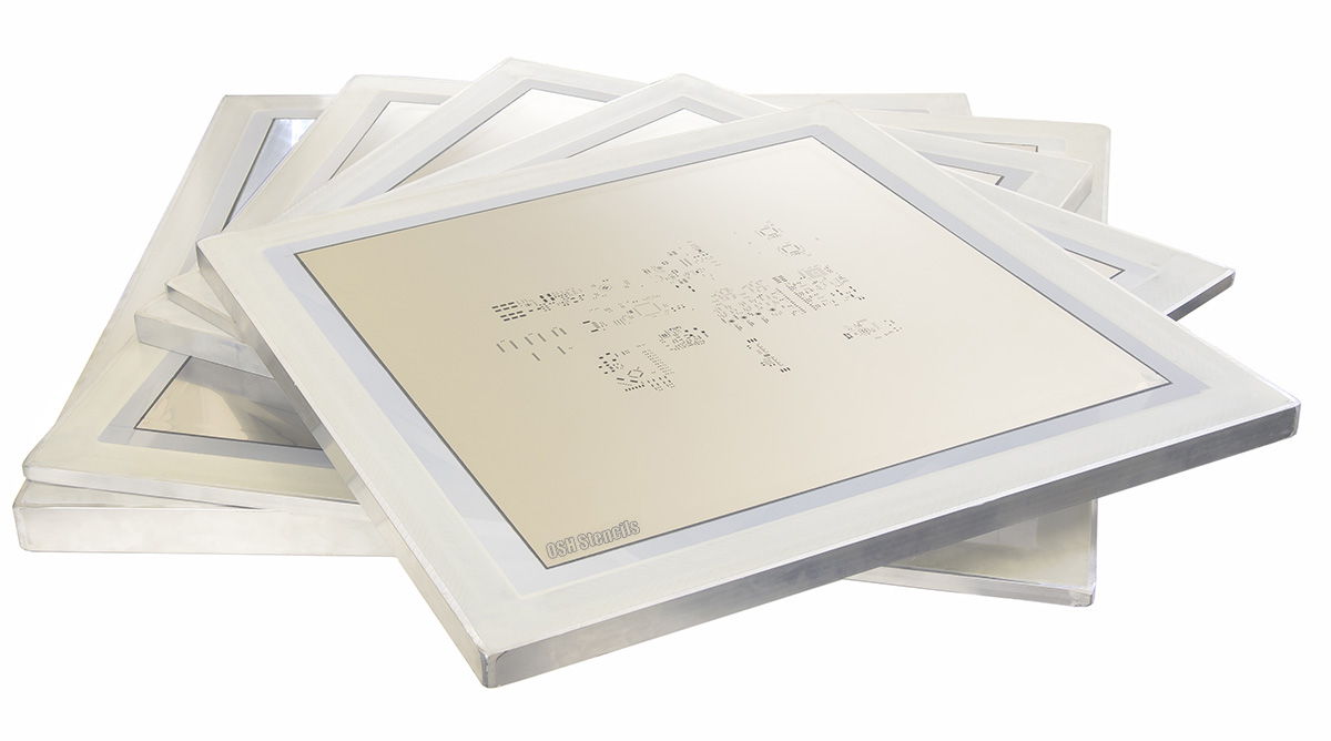
All of our SMT Stencils are 100% laser-cut type 304 full-hard stainless steel, ensuring the finest quality finish on the market today. We use a .001" laser beam with 98% overlap creating an extremely smooth hole that provides the best paste release. Most stencil fabricators use a .003" laser leaving mouse bites on the aperture edge. You can choose a PCB Prototype stencil, a frameless foil stencil, or a rigid permanently mounted stencil. Both the frameless and framed stencils come in various sizes to accommodate your printer and stencil requirements.
PCB Stencil Types Available:
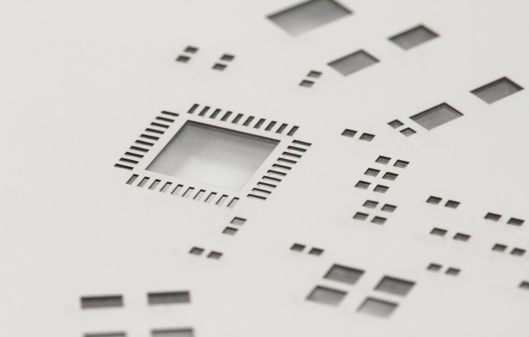
1. Laser-cut stencils
The openings are lasered on 100% stainless steel. Generally speaking, this kind of stencil can be produced with high quality and a high degree of precision within a short time.
- Advantages: high accuracy; barely influenced by objective elements; trapezoid opening beneficial for demoulding; suitable for accurate cutting; reasonable price;
- Disadvantages: relative low manufacturing speed.
2. Chemical-etch stencil
The openings are etched into the metal using acid. Usually this kind of stencil offers better protection on material temper and hardness.
- Advantages: one-time formation; relatively high manufacturing speed; low cost;
- Disadvantages: tending to form sand clock shape or large openings; numerous manufacturing stages and accumulating errors; unsuitable for fine pitch stencils; bad for environmental protection.
3. Prototype PCB Stencil (Low-volume manual printing. Ideal for prototypes)
When prototyping dictates fast action with minimal cost, our prototype stencils are the best solution. Prototype Stencils gives you a quality stencil and framework so you can handle assembly from the convenience of your own desk.
Prototype SMT Stencil Features:
- Eliminate the registration difficulty associated in hand printing with a flat piece of metal
- Eliminate printer set up for short run prototypes
- Allow quick alignment for repeatability
- Save money over full size stencils designed for automated printers<
- Squeegee included
| Prototype SMT Stencil Specs: | |
| Technology | 100% laser cut |
| Material Used | Stainless Steel |
| Stencil Thickness | 0.06 ~ 0.3 mm |
| Minimum Cut Width | 0.05 mm |
| Maximum Size | 736 X736 mm |
| Aperture Tolerance | within 0.007mm |
| Allow for Fiducial Data | Yes |
| Delivery | 1 ~2 Day |
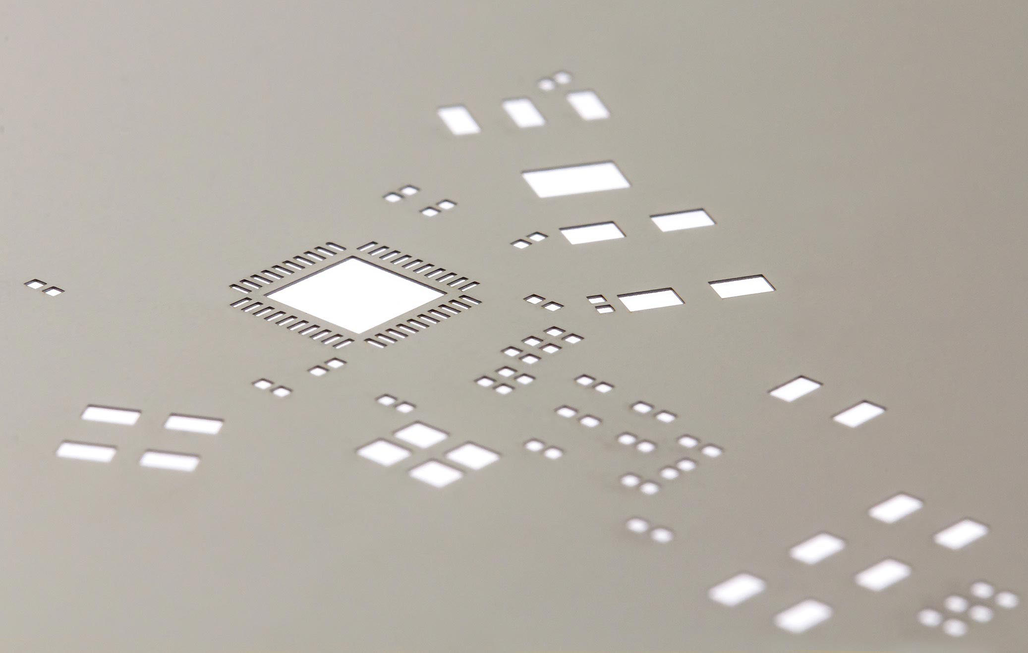
4. NEW Prototype PCB Stencil Kit (with leaded or lead/free solderpaste)
Includes Prototype Stencil, one board holder, leaded or lead-free solder paste (must specify), temperature marker, squeegee, ESK-safe gloves and alcohol wipe.
5. NEW Pick and Place Tool
Handy and convenient for low quantity prototype assembly using the Prototype Stencils. Re-usable, includes vacuum bulb and vacuum clips with diameters of 3/8", 1/4", and 1/8".
6. Framed SMT Stencils (Also called "Glue-in" or Mounted Stencils)
Framed stencils are laser-cut stencils designed for high volume screen-printing. With a framed stencil, your stencil is securely mounted to either a cast or extruded aluminum stencil frame a stencil frame using a mesh border, allowing for complete control.
Framed SMT Stencil Features:
- Unique Process for smooth aperture walls
- ery clean laser-cut apertures
- Excellent print performance
- Excellent for high-volume stencil printing on printed circuit boards
- Unique process creates permanent non-removable non-fading fiducial
- All framed SMT stencils are double bonded to extreme wear
- 24-hour turnaround standard
| Framed SMT Stencil Specs: | |
| Technology | 100% laser cut |
| Material Used | Stainless Steel |
| Frame Types | Cast, Space Saver |
| Stencil Thickness | 0.06 ~ 0.3 mm |
| Minimum Cut Width | 0.05 mm |
| Maximum Size | 736 X736 mm |
| Aperture Tolerance | within 0.007mm |
| Allow for Fiducial Data | Yes |
| Allow for Panelized Data | Yes |
| Delivery | 1 ~2 Day |
Framed PCB Stencil Specification
|
Framed PCB Stencil Area |
Maximum Squeegee Area |
|
300mm*400mm (11.81inch*15.75inch) |
120mm*220mm (4.72inch*8.66inch) |
|
370mm*470mm (14.57inch*18.5inch) |
200mm*300mm (7.87inch*11.81inch) |
|
400mm*600mm (15.75inch*23.62inch) |
220mm*400mm (8.66inch*15.75inch) |
|
400mm*700mm (15.75inch*27.56inch) |
220mm*500mm (8.66inch*19.69inch) |
|
400mm*800mm (15.75inch*31.5inch) |
220mm*600mm (8.66inch*23.62inch) |
|
400mm*900mm (15.75inch*35.43inch) |
220mm*700mm (8.66inch*27.56inch) |
|
400mm*1000mm (15.75inch*39.37inch) |
220mm*800mm (8.66inch*31.5inch) |
|
400mm*1200mm (15.75inch*47.24inch) |
220mm*1000mm (8.66inch*39.37inch) |
|
400mm*1400mm (15.75inch*55.12inch) |
220mm*1200mm (8.66inch*47.24inch) |
|
420mm*520mm (16.54inch*20.47inch) |
240mm*340mm (9.45inch*13.39inch) |
|
450mm*550mm (17.72inch*21.65inch) |
270mm*370mm (10.63inch*14.57inch) |
|
500mm*800mm (19.69inch*31.5inch) |
320mm*600mm (12.6inch*23.62inch) |
|
500mm*1200mm (19.69inch*47.24inch) |
320mm*1000mm (12.6inch*39.37inch) |
|
550mm*650mm (21.65inch*25.59inch) |
340mm*440mm (13.39inch*17.32inch) |
|
584mm*584mm (23inch*23inch) |
380mm*380mm (15inch*15inch) |
|
736mm*736mm (29inch*29inch) |
480mm*480mm (19inch*19inch) |
7. Frameless SMT Stencil - Foil/Plate Only (for universal frames)
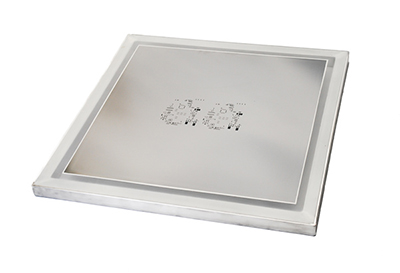
Foil or Plate Only stencils are designed to work within interchangeable plate or "universal" systems. Also referred to as "reusable", these stencils do not need to be permanently glued into a frame.
Frameless SMT Stencils also referred to as foils are laser cut solder paste stencils designed to work with stencil tensioning systems known as reusable stencil frames. This type of stencil does not need to be permanently glued in a frame. Frameless stencils are significantly less expensive than framed stencils and provide money-saving storage while still delivering superior quality and performance.
Frameless SMT Stencil Features:
- Reduced storage space requirements
- Significantly less expensive than framed stencils
- Excellent for prototype Printed Circuit Board Assembly or short runs
- Smooth aperture walls, can be used for 16 Mil pitch and below and for Micro BGA's
- 24-hour turnaround standard
| Frameless SMT Stencil Specs: | |
| Technology | 100% laser cut |
| Material Used | Stainless Steel |
| Stencil Thickness | 0.06 ~ 0.3 mm |
| Minimum Cut Width | 0.05 mm |
| Maximum Size | 280 X 380 mm |
| Allow for Fiducial Data | Yes |
| Allow for Panelized Data | Yes |
| Delivery | 1 ~2 Day |
8. Frameless SMT Stencil - Foil/Plate Only (for hand printing)
For times when you need precise control for smaller production runs, our Foil or Plate Only stencils are ideal. These frameless stencils allow you to hand print with precision just the amount you need and can be stored conveniently.
9. Electroformed SMT Stencils
Electroformed SMT stencils are nickel-based, electroform foils permanently mounted in a stencil frame using a mesh border to tightly stretch the stencil foil taut in the frame. Electroformed stencils offer the best paste release characteristics available and are frequently used for fine pitch (20 mil to 12 mil pitch) SMT applications on printed circuit boards. They are also used for µBGA's, Flip Chip, and Wafer Bumping (12 mil to 6 mil pitch).
Electroformed SMT Stencil Features:
- The smooth trapezoidal sidewalls of an electroformed stencil allow for better paste release
- Nickel has a lower coefficient of friction compared to stainless steel
- Electroform foils are harder than full hard stainless steel of comparable thickness, providing for longer stencil life
- 24-hour turnaround standard
| Electroformed SMT Stencil Specs: | |
| Technology | Electroforming |
| Material Used | Nickel |
| Suitable Applications | All Component Pitches |
| Aperture Tolerance | within 0.007mm |
| Stencil Thickness | 0.06 ~ 0.3 mm |
| 0.06mm.0.08mm.0.1mm.0.12mm.0.13mm.0.15mm.0.18mm.0.2mm.0.3mm | |
| Positional Accuracy | ± 0.008mm |
| Delivery | 1 ~2 Day |
What's the difference between a framed stencil and a frameless stencil?
A framed PCB stencil will have a 0.5" to 1.5" thick metal frame around it, similar to a picture frame. Framed stencils are often used by contract manufacturers, assembly and board houses, and large scale production facilities and are commonly placed in a manual or automated stencil printing machine. Frameless stencils are a thin sheet of material cut with a small border around your design. For example pictures on these products, please visit our Gallery.
What's the difference between Polyimide and Stainless Steel?
All stencils are made with high quality Polyimide and Stainless Steel. We use only the industry leading Stainless Steel, designed specifically for stencils. These materials are ideal for prototype or Multilayer PCB .
Stainless Steel: 0.0007" Laser spot size, 0.001" minimum aperature size.
Polyimide Film: 0.003" Laser spot size, 0.005" minimum aperature size.
Polyimide has a lower precision rate due to the way it is processed and its ability to withstand heat during the cutting process. Minor variances will occur when the material reacts to the laser. Paste release is great, but this material should be limited to a small number of uses and with components 0402 or bigger.
The minimum aperature size for Polyimide is 0.005" vs 0.001" for Stainless Steel. Polyimide also has a natural curl in the material caused by the way the film is manufacturered, this is outside of our control. Stainless Steel provides the ultimate in precision and quality, with a 0.0007" spot size, and exceptional paste release with a truly flat surface. If you want the absolute best reflow experience, there is no comparison, Stainless Steel is the superior material.
Analysis and Treatment of Common Problems in PCB SMT stencil
- Insufficient solder paste
- Smudging/bridging
- Misalignment print
- Bow and twist
How to Determine Stencil Size?
Stencil size is composed by two parts: internal size and overall size. Internal size is the size compatible with that of PCB ready to be assembled while overall size refers to the size compatible with printer parameter limit. As long as both sizes are accurately designed, stencil will be able to make full use of its functions.
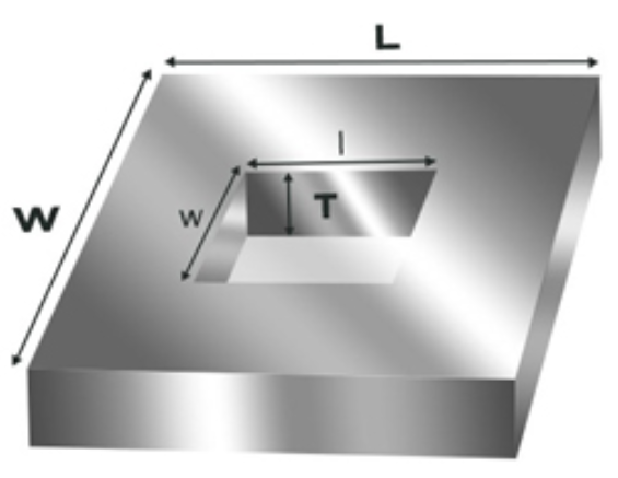
Internal size of stencil can be figured out conforming to the following rule:
- Width of Framed Stencil = width of PCB + 100mm while its Length = length of PCB + 100mm
- Width of Frameless stencil = width of PCB + 200mm while its Length = length of PCB + 200mm
For example, if one circuit board size is 50*50mm, then the size of its framed stencil should be around 150*150mm and the size of its frameless stencil should be around 250*250 mm.
It's easy to remember and operate so it worked for manual solder paste printing in SMT assembly prior to the advent of automatic printer. It can be said that different PCB sizes lead to generations of different internal sizes of stencil.
When it comes to automatic solder paste printer, however, it's relatively solid. Overall size of stencil has to be determined by parameter limit of the equipment, that is, printer, because stencil has to work within the range of printer with a frame. Different printers feature different parameter regulations. As far as PCBCart is concerned, the stencil size compatible with our printer can be either 650mm*650mm or 736mm*736mm.
PCB designers have to focus on internal size of stencil, they don't need to care about its overall size since it is generally determined by the parameters of printer in your contract assembler workshop.
How to Use PCB SMT Stencils?
PCB Stencil
PCB Stencil,SMT Stencil,SMD Stencil,Laser Stencil
JingHongYi PCB (HK) Co., Limited , https://www.pcbjhy.com