12.2.6 PicoBlaze Input/Output Port
The PicoBlaze microcontroller supports up to 256 inputs and 256 outputs. PicoBlaze's input and output related signals are detailed in the "PicoBlaze Microcontroller Interface Signals" section, including PORT_ID[7:0], IN_PORT[7: 0], OUT_PORT[7:0], READ_STROBE WRITE_STROBE. In timing-critical designs, two clock cycles are allowed for PORT_ID and data paths, and one clock cycle is required for READ_STROBE and WRITE_STROBE. To improve performance, the pipeline registers can be inserted if allowed.
PORT_ID: This signal is used as the identifier or address of the input or output port. Its active high level lasts for two clock cycles. The purpose of this is to have enough time for decoding, enough time to connect to the asynchronous RAM, and, in the case of two-cycle operation, to allow slave synchronous RAM (eg , BRAM) read data.
The INPUT and OUTPUT operations support direct and indirect addressing, and the port address is specified by an immediate value or by a register. Indirect addressing is suitable for accessing BRAM, peripherals with contiguous addresses, tables in on-chip or off-chip memory.
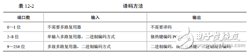
Extending the PicoBlaze peripheral is actually very convenient, and the only challenge is how to decode the PORT_ID with minimal logic resources. Table 12-2 shows the general method (depending on the number of ports).
The input operation transfers the data of the IN_PORT input to any of the 16 data registers specified by register sX, as shown in Figure 12-11. PORT_ID is determined by sY or is determined by an 8-bit immediate value specifying the input source. The input source is selected by a multiplexer whose size is proportional to the number of channels of the input source, which directly affects the performance of the PicoBlaze.

Figure 12-11 Input Operation and FPGA Internal Interface
Figure 12-12 shows the timing diagram of the input instructions. The figure shows that the PicoBlaze microcontroller reads data from the port specified by s7 and the data is read into s0. When this instruction is executed, the contents of register s7 appear on PORT_ID, PORT_ID is decoded by the internal logic of the FPGA, and the requested data appears in IN_PORTREAD_STROBE. It becomes higher during the second clock cycle of the input instruction, although READ_STROBE is mainly used for FIFO. Enables the FIFO to update its read pointer. The data appearing in IN_PORT is sampled on the second rising edge, indicating that the INPUT instruction has been executed, after which the data is sampled into s0.
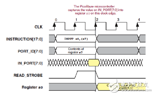
Figure 12-12 PORT Timing of the INPUT Instruction
As can be seen from the timing diagram in Figure 12-12, since the PORT_ID is valid for two clock cycles, the input data multiplexer can be registered to ensure performance, as shown in Figure 12-13.
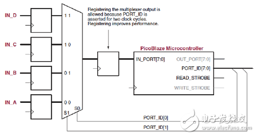
Figure 12-13 Converting multiple inputs to one input by a multiplexer
Second, the OUTPUT operationThe output operation sends the contents of register sX to OUT_PORT, which is determined by register sY or by an 8-bit immediate value, specifying the output. WRITE_STROBE indicates that the OUT_PORT data is valid and ready to be captured. Normally, WRITE_STROBE and PORT_ID combine clock enable or write enable for FPGA logic to capture output data.
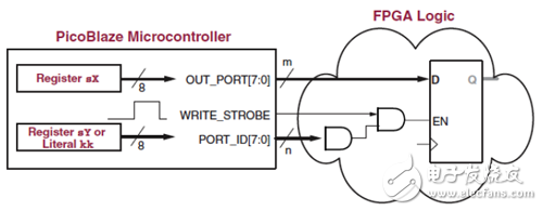
Figure 12-14 OUT_PORT and FPGA Logic
Figure 12-14 shows an example of an extended output port. Figure 12-15 shows its timing diagram. PicoBlaze sends the contents of s0 to the port with PORT_ID 65HEX, the content of s0 appears in OUT_PORT, and the port address 65HEX appears in PORT_ID, WRITE_STROBE The second clock edge of the instruction cycle goes high, indicating that the data is valid.
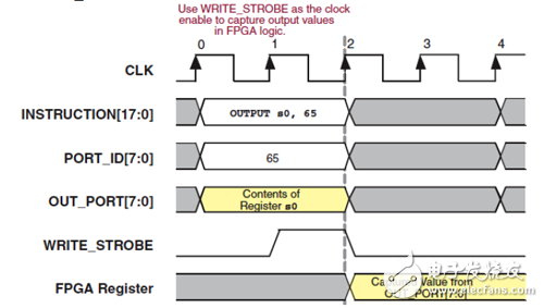
Figure 12-15 PORT Timing of the OUT_PORT Instruction
For 8 or less output ports, one-hot encoding is commonly used, as shown in Figure 12-16, because it only needs to decode a bit of PORT_ID, so FPGA translation is greatly reduced. Code logic requires resources while also improving performance. If the number of PORT_ID bits used for decoding is 3 or less, the decoding logic can be implemented with only one level of logic, and the performance is highest at this time.
Figure 12-17 shows a simple output program that defines four output ports with one-hot encoding. At the same time, a broadcast output port is defined. Four different values ​​are output to the four output ports. The last two are shown. The statement clears all 4 ports.
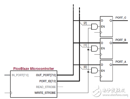
Figure 12-16 Simple output
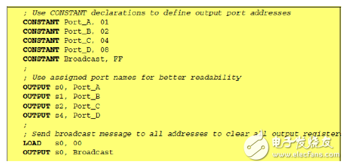
Figure 12-17 One-hot addressing output routine
FORD Oil Filter
FORD Oil Filter
Zhoushan Shenying Filter Manufacture Co., Ltd. , https://www.renkenfilter.com