Abstract: In order to reduce cost and improve design flexibility, an FPGA-based 1553B bus interface scheme is proposed. Based on the top-down design method, based on the analysis of the working principle and response process of the 1553B bus interface, the interface schemes are completed. FPGA function module design; write VHDL code for key modules, and use AcTIveâƒHDL software for simulation; use Virtexâƒ5 FPGA development board and PC as verification platform, simulate BC and RT respectively in FPGA, under PC command The transmission and reception tests between the BC and RT function modules have been carried out. The results show that the system can operate stably at the 1 MHz data rate specified by the protocol. At the same time, in order to improve the interface performance, the optical fiber is used instead of the traditional cable transmission medium, and the RockeTIO core embedded in the FPGA is used. The optical transmission of the traditional 1553 protocol data can reach a rate of more than 3 Gb/s.
0 Preface
MILâƒSTDâƒ1553B (Digital Time Division Command/Response Multiplex Data Bus) was proposed by the US Department of Defense in the late 1970s. It uses Manchester encoding and redundant bus topology, which is very good. The clock synchronization capability and fault tolerance mechanism greatly simplify the interconnection between electronic devices, and thus are widely used in military, aerospace, aerospace and other fields with high reliability requirements.
With the superior performance of the 1553B bus, the application requirements of related fields in China are increasing, and its key position is increasingly prominent. However, due to the complexity of the 1553B protocol and the relative backwardness of domestic technology, most of the 1553B bus designs use foreign protocol interface chips, such as Dâƒ's BUâƒ61580. On the one hand, such chips are not only expensive, but also vulnerable to foreign restrictions; on the other hand, in practical applications, many functions of the chip are slightly redundant and cannot be flexibly designed.
Field Programmable Gate Array FPGAs integrate a large amount of logic into a single IC. The internal resources are abundant, and the corresponding EDA development tools are powerful. It is an ideal system for system design and implementation. FPGA has many advantages such as short development cycle, low cost and high flexibility. Based on the analysis of protocol specifications, it is feasible to implement MILâƒSTDâƒ1553B bus interface through FPGA. This paper proposes an FPGA-based 1553B bus interface design scheme, and writes VHDL code for simulation. Finally, the design verification is completed on the FPGA, and the 1 Mb/s cable transmission and the 3 Gb/s optical fiber of the traditional 1553B protocol data are realized. transmission.
MILâƒSTDâƒ1553B is a command/response multiplex bus that uses a redundant bus structure to immediately switch to a redundant transmission line in the event of a current transmission line failure, preventing communication interruptions. At the same time, the 1553B protocol strictly defines the message format, limits the maximum transmission data amount of each message and the maximum response time of the bus unit, and standardizes the bus coupling mode, cable electrical characteristics, etc., ensuring high reliability of bus transmission from various aspects. .
The 1553B bus contains three types of bus units: a bus controller BC, a remote terminal RT, and a bus monitor MT, each unit communicating in an orderly manner under the scheduling of the bus controller BC. Data on the bus is transmitted in word-based units and is divided into command words, status words, and data words, each of which contains 20 bits. Each data exchange between bus units is called a message, and the 1553B protocol specifies 10 message formats. Otherwise, the messages in other formats are illegal messages. The bus adopts Manchester coding mode, which is convenient for the receiving end to extract the synchronous clock and simplify the bus structure.
2 1553B bus interface overall designThe bus interface is a data exchange medium between the external system and the bus, and its main function is to complete the processing of the bus protocol. According to the characteristics of the 1553B protocol, the overall design of the bus interface is shown in Figure 1.
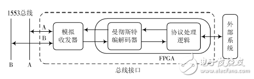
Figure 1 bus interface overall design
As can be seen from Figure 1, the bus interface includes three modules: analog transceiver, Manchester codec and protocol processing logic. The analog transceiver completes the level conversion between the FPGA output signal and the bus signal, and can be completed by a dedicated conversion chip, and the Manchester codec and the 1553B protocol processing logic are the main components of the interface, and the data encoding and decoding and protocol processing are completed. Implemented by FPGA. The bus interface is connected to an external system via a certain address, data and handshake signal.
3 Manchester codec module design3.1 1553B bus data format signal coding and decoding design is determined by the characteristics of the bus transmission layer, 1553B message word format and Manchester code pattern shown in Figure 2.
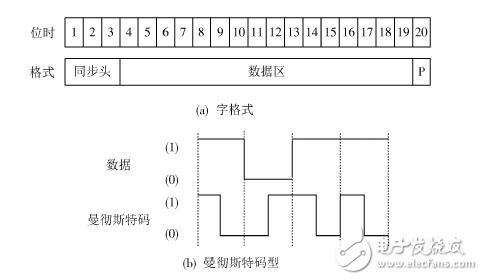
Figure 2 1553B message word format and Manchester pattern
The 1553B bus transmits data in units of words. Each word contains 20 bits, of which the first 3 bits are sync headers and the last 17 bits are data bits and parity bits, as shown in Figure 2(a). The bus data transmission rate is 1 Mb/s, using Manchester II bi-phase code encoding, each data has a transition edge in between, and the positive to negative transition indicates logic '1', from negative to positive transition. Indicates logic '0', and its pattern correspondence is shown in Figure 2(b).
3.2 Encoder design
The design of the encoder is relatively simple, mainly completing the Manchester encoding of the message word to be sent, and converting it and outputting it in parallel. Since the Manchester code has a transition in the middle of each bit of data, each bit needs to be split into two bits and sent separately. Its working process is:
(1) Synchronization header coding, if it is a data word synchronization header, the code is "111000" (from high to low, the same below), if it is status word or command word synchronization header, the code is "000111";
(2) Data and parity bit coding, if it is '0', the code is "10", if it is '1', the code is "01";
(3) The encoded 40-bit data is serially output in descending order.
The FPGA uses a 16 MHz master clock. Since each bit of data after encoding corresponds to 0.5 μs, the main clock is divided to generate a 2 MHz clock to control the encoder to transmit 40 bits of data. One bit is sent on each clock edge, which just satisfies 1553B bus 1 The rate requirement for Mb/s [5].
3.3 decoder design
The decoder mainly completes the decoding of the message word, and converts the string and outputs it. The working process is as follows:
(1) The active level on the bus is detected and the decoder starts to work;
(2) Synchronization header decoding, detecting that the instruction word and the status word synchronization header are represented by "011", and detecting that the data word synchronization header is represented by "100";
(3) 16-bit data bits and 1-bit parity bits are decoded;
(4) The decoded message word (20 bits) is output in parallel.
The synchronization header and data bit detection are shown in Figure 3.
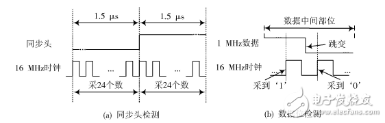
Figure 3 sync header and data bit detection
According to the 1553B protocol, when the sync header contains three bits, there is a jump at 1.5 bits. As shown in Figure 3(a), after the synchronization header arrives, the decoder continuously acquires 48 numbers. In theory, the 16 MHz clock is used. If 24 '0's and 24 '1's are detected, it means that it is valid. Synchronization header, but considering the factors such as signal rise time and fall time, if 22 or 23 '0' and '1' are actually detected, it can be determined that the synchronization header is valid and the next data is received.
When the data bit contains one bit, there is a jump at 0.5 bits. As shown in Figure 3(b), in the middle of each data, if the previous clock is sampled to '0' and the next clock is sampled to '1', the current data bit is '0', otherwise it is '1'. '. In addition, if the number captured does not jump, it is all '0' or all '1', an error flag is generated, and the protocol processing logic or subsystem is notified to perform corresponding error processing.
4 protocol processing module design4.1 Protocol Processing Module Response Process
The protocol processing module implements the protocol processing of the three bus terminals BC, RT and MT. Before the FPGA module design, the response flow in the three working modes of the protocol processing module is analyzed and designed according to the 1553B protocol.
4.1.1 BC mode
BC (Bus Controller) is the core of the 1553B bus, from which any type of data exchange on the bus is initiated. The interface response flow design in BC mode is shown in Figure 4.
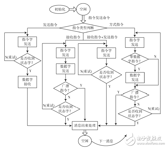
Figure 4 Interface response process in BC mode
The bus instructions specified by the MILâƒSTDâƒ1553B protocol can be divided into three types: send command, receive command and mode command. Four types of functions can be realized: RT to BC data transmission, BC to RT data transmission, RT to RT. Data transfer and bus management. According to Figure 4, the main working process of the interface in BC mode is:
(1) Send the corresponding command word according to the requirements of the external system to initiate the bus transmission;
(2) According to the different types of instructions, enter different response processes, including data word transmission, data word reception and status word reception;
(3) After the message is completed, the message end processing is performed, mainly including the generation of the message end flag, error processing, and judging the state of the bus terminal according to the received RT status word.
It should be noted that if BC does not receive an RT status response within the specified time, it needs to resend the command word for retry.
4.1.2 RT mode
RT (Remote Terminal) is an instruction/response terminal on the 1553B bus. It responds to commands sent by BC, receives or transmits data as required, returns status words within a specified time, and obeys BC bus management. The interface response process design in RT mode is shown in Figure 5.
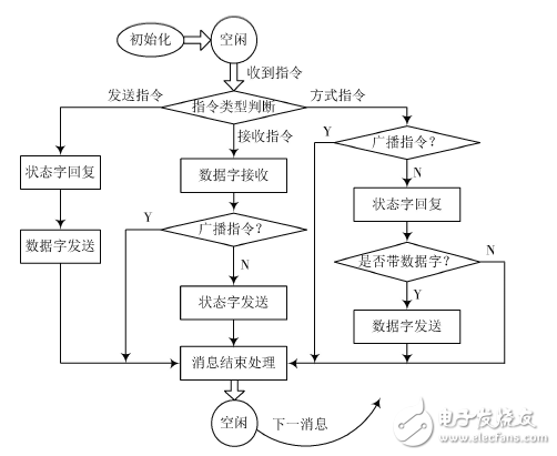
Figure 5 Interface response process in RT mode
According to Figure 5, the main working process of the interface in RT mode is:
(1) After receiving the command word, the instruction analysis is performed, and the corresponding response flow is entered according to the instruction type;
(2) Receiving, sending, and replying to the status word according to the process;
(3) After the message is completed, the message end processing is performed, mainly including the generation of the message end flag, the error processing, and the generation of the mode flag under the special mode instruction.
The product is used for cutting reinforced concrete, granite quarry and marble
sawing wire, sawing wire rope, wire rope for cutting, wire rope for marble cutting, wire rope for stone cutting
ROYAL RANGE INTERNATIONAL TRADING CO., LTD , https://www.royalrangelgs.com