Basic principles of DDS architecture
With the widespread use of digital technology in instrumentation and communication systems, digital control methods that generate multiple frequencies from a reference frequency source have been born, namely direct digital frequency synthesis (DDS). The basic structure is shown in Figure 1. The simplified model uses a stable clock to drive a programmable read only memory (PROM) that stores one or more integer cycles of a sine wave (or other arbitrary waveform). As the address counter progressively executes each memory location, the corresponding signal digital amplitude at each location drives the DAC, which in turn produces an analog output signal. The spectral purity of the final analog output signal is primarily dependent on the DAC. The phase noise is mainly from the reference clock.
DDS is a sampled data system, so all sampling-related issues must be considered, including quantization noise, aliasing, filtering, and so on. For example, higher-order harmonics of the DAC output frequency are folded back to the Nyquist bandwidth and are therefore not filterable, while higher-order harmonics of the PLL-based synthesizer can be filtered. In addition, there are several other factors to consider, which will be discussed later.
Figure 1: The basic principle of a direct digital frequency synthesis system
The basic problem with this simple DDS system is that the final output frequency can only be achieved by changing the reference clock frequency or reprogramming the PROM, which is very inflexible. The actual DDS system uses a more flexible and efficient way to achieve this, using a digital hardware called a numerically controlled oscillator (NCO). Figure 2 shows a block diagram of the system.
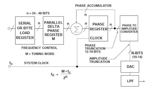
Figure 2: Flexible DDS System
At the heart of the system is a phase accumulator whose contents are updated every clock cycle. Each time the phase accumulator is updated, the digital word M stored in the delta phase register is added to the number in the phase register. Assuming that the number in the delta phase register is 00...01, the initial content in the phase accumulator is 00...00. The phase accumulator is updated every 00...01 every clock cycle. If the accumulator is 32 bits wide, then 232 (more than 4 billion) clock cycles are required before the phase accumulator returns to 00...00, and the cycle repeats.
The truncated output of the phase accumulator is used as the address of the sine (or cosine) lookup table. Each address in the lookup table corresponds to a phase point of the sine wave from 0° to 360°. The lookup table includes the corresponding digital amplitude information for a complete sine wave period. (Actually, only 90° of data is needed because the two MSBs contain orthogonal data). Therefore, the lookup table maps the phase information of the phase accumulator to the digital amplitude word, which in turn drives the DAC. Figure 3 shows this with a graphical "phase wheel".
Consider the case where n = 32 and M = 1. The phase accumulator will progressively execute each of the 232 possible outputs until it overflows and resumes. The corresponding output sine wave frequency is equal to the input clock frequency of 232. If M = 2, the phase accumulator register is "rolled" at twice the speed and the output frequency is doubled. The above can be summarized as follows:
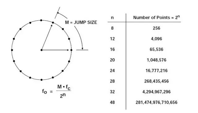
Figure 3: Digital Phase Wheel
An n-bit phase accumulator (in most DDS systems, n typically ranges from 24 to 32) there are 2n possible phase points. The digital word M in the Δ phase register represents the number of increments per phase of the phase accumulator. If the clock frequency is fc, the output sine wave frequency is calculated as:
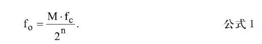
This formula is called the DDS "tuning formula". Note that the frequency resolution of the system is equal to fc/2n. When n = 32, the resolution is over 4 billion! In an actual DDS system, the bits of the overflow phase register do not enter the lookup table, but are truncated, leaving only the first 13 to 15 MSBs. This reduces the size of the lookup table without affecting the frequency resolution. Phase truncation only adds a small amount of acceptable phase noise to the final output. (See Figure 4).
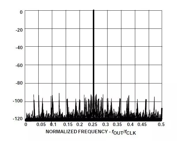
Figure 4: The calculated output spectrum shows 90 dB SFDR at 15-bit phase truncation
The resolution of the DAC is typically 2 to 4 bits less than the width of the lookup table. Even a perfect N-bit DAC increases the quantization noise of the output. Figure 4 shows the output spectrum calculated for a 15-bit phase accumulator with a 15-bit phase cut. When the M value is selected, the output frequency will shift slightly from 0.25 times the clock frequency. Note that both phase truncation and finite DAC resolution produce spurs that are at least 90 dB lower than the full-scale output. This performance goes far beyond any commercial 12-bit DAC, enough for most applications.
The basic DDS system described above is extremely flexible and has high resolution. Simply change the contents of the M register and the frequency can be changed immediately without phase discontinuity. However, the actual DDS system first needs to perform a serial or byte load sequence to load the new frequency word into the internal buffer register and then load the M register. This will minimize the number of package pins. After the new frequency word is loaded into the buffer register, the parallel output Δ phase register is synchronized, changing all bits simultaneously. The number of clock cycles required to load the delta phase buffer register determines the maximum rate of change of the output frequency.
Aliasing in DDS systems
An important output frequency range limitation may occur in a simple DDS system. The Nyquist criterion states that the clock frequency (sampling rate) must be at least twice the output frequency. The actual maximum output frequency is limited to approximately 1/3 of the clock frequency range. Figure 5 shows the DAC output in a DDS system with an output frequency of 30 MHz and a clock frequency of 100 MHz. As shown, the DAC must be followed by an anti-aliasing filter to eliminate the lower image frequency (100 – 30 = 70 MHz).

Figure 5: Aliasing in a DDS system
Note that the amplitude response of the DAC output (before filtering) is followed by a sin(x)/x response, which is zero at the clock frequency and its integer multiple. The exact calculation formula for the normalized output amplitude A(fO) is as follows:

Where fO is the output frequency and fc is the clock frequency.
The reason for this roll-off is because the DAC output is not a series of zero-width pulses (as in the best resampler), but a series of rectangular pulses with a width equal to the reciprocal of the update rate. The magnitude of the sin(x)/x response is 3.92 dB lower than the Nyquist frequency (1/2 of the DAC update rate). In fact, the anti-aliasing filter's transfer function can be used to compensate for the sin(x)/x roll-off, making the overall frequency response relatively flat, reaching the maximum output DAC frequency (typically 1/3 update rate).
Another important consideration is that, unlike PLL-based systems, the high-order harmonics of the fundamental output frequency in the DDS system are folded back to the baseband due to aliasing. These harmonics cannot be removed by the anti-aliasing filter. For example, if the clock frequency is 100 MHz and the output frequency is 30 MHz, the second harmonic of 30 MHz will appear at 60 MHz (out-of-band), but it will also appear at 100 – 60 = 40 MHz (aliasing) . Similarly, the third harmonic (90 MHz) will appear in the band with a frequency of 100 – 90 = 10 MHz and the fourth harmonic will occur at 120 – 100 MHz = 20 MHz. Higher-order harmonics also fall within the Nyquist bandwidth (DC to fc/2). The positions of the first 4 harmonics are shown in the figure.
DDS system used as an ADC clock driver
DDS systems such as the AD9850 provide an excellent way to generate an ADC sample clock, especially when the ADC sample frequency must be software controlled and locked to the system clock (see Figure 6). The DAC output current, IOUT, drives a 200 Ω, 42 MHz low-pass filter with source and load impedance terminations and an equivalent load of 100 Ω. The filter eliminates spurious frequency components above 42 MHz. The filtered output can drive an input to the internal comparator of the AD9850. The DAC compensates for the output current to drive a 100 Ω load. The 100 kΩ resistor divider output between the two outputs is decoupled to produce a reference voltage for use by the internal comparator.
The comparator output has a 2 ns rise and fall time that produces a square wave compatible with TTL/CMOS logic levels. The jitter at the output edge of the comparator is less than 20 ps rms. Output and compensation outputs are available on request.
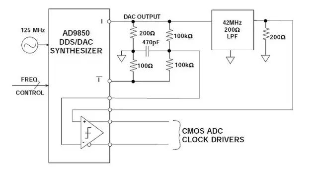
Figure 6: Using a DDS System as an ADC Clock Driver
In the circuit shown in Figure 6, the total output rms jitter of the 40 MSPS ADC clock is 50 ps rms, and the resulting signal-to-noise ratio degradation must be considered in wide dynamic range applications.
Amplitude modulation in DDS systems
Amplitude modulation in a DDS system can be achieved by placing a digital multiplier between the lookup table and the DAC input, as shown in Figure 7. Another way to modulate the output amplitude of the DAC is to change the reference voltage of the DAC. In the AD9850, the internal reference control amplifier has a bandwidth of approximately 1 MHz. This method is very effective in the case where the output amplitude changes relatively small, as long as the output signal does not exceed the specification of +1 V.

Figure 7: Amplitude Modulation in a DDS System
Spurious-free dynamic range considerations in DDS systems
In most DDS applications, the primary consideration is the spectral purity of the DAC output. Unfortunately, the measurement, prediction, and analysis of this performance is complex and involves a large number of interaction factors.
Even an ideal N-bit DAC produces harmonics in the DDS system. The magnitude of these harmonics is primarily determined by the ratio of the output frequency to the clock frequency. The reason is that the spectral component of the DAC quantization noise varies with the ratio, although its theoretical rms value is still equal to q/√12 (where q is the weight of the LSB). The assumption that quantization noise behaves as white noise and is evenly distributed over the Nyquist bandwidth is not applicable in DDS systems (this assumption is more applicable in ADC systems because the ADC adds some noise to the signal, Thus "disturbing" the quantization error or randomizing it. However, there is still a certain correlation). For example, if the DAC output frequency is accurately set to a divisor of the clock frequency, the quantization noise is concentrated at a multiple of the output frequency, that is, primarily depending on the signal. If the output frequency is slightly out of tune, the quantization noise becomes more random, improving the effective SFDR.
Figure 8 illustrates the above scenario where a 4096 (4k) point FFT is calculated based on digitized data from an ideal 12-bit DAC. In the chart (A) on the left, the ratio of the selected clock frequency to the output frequency is exactly equal to 40, and the obtained SFDR is about 77 dBc. In the chart on the right, the ratio is slightly out of tune and the effective SFDR increases to 94 dBc. In this ideal case, the SFDR is changed by 17 dB with only a slight change in the frequency ratio.
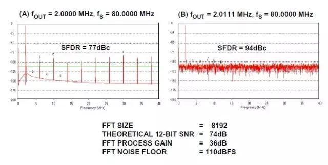
Figure 8: Effect of clock to output frequency ratio on theoretical 12-bit DAC SFDR with 4096-point FFT
Therefore, by carefully selecting the clock and output frequency, the best SFDR can be obtained. However, in some applications, this may be difficult to achieve. In an ADC-based system, adding a small amount of random noise to the input may randomize the quantization error and reduce this effect. The same effect can be achieved in the DDS system, as shown in Figure 9. The pseudo-random digital noise generator output is first added to the DDS sine amplitude word and then loaded into the DAC. The amplitude of the digital noise is set to around 1/2 LSB. This allows the randomization process to be achieved at the expense of a slight increase in the overall output noise floor. However, in most DDS systems, there is enough flexibility to choose different frequency ratios, so no disturbance is required.
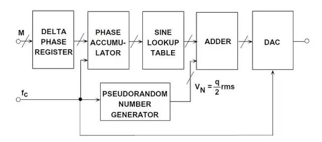
Figure 9: Injecting digital perturbations into the DDS system to randomize quantization noise and improve SFDR
In many electronic communication equipment and instruments where always use some cable assemblies to connect some electronic units and circuits.
We use different connectors, such as SMB, SMA, N TNC, MCX, IPEX, BNC with different cables such as Flexible cable, semi-flexible cable, semi-rigid cable, corrugated cable etc. Our products widely used in customers' special technology, equipment, skilled operation , advanced test
We test all the finished cable assemblies one by one, Insulation resistance , Dielectric Withstanding Voltage and VSWR at the frequency range form 0~18 GHz. to meet clients' requirements and Characteristic.
RF Connector Coaxial Cable,RF Cable Assembly,SMA Cable Assemblies,N Type Cable Assemblies
Xi'an KNT Scien-tech Co., Ltd , https://www.honorconnector.com