The mixer is the core module in the wireless transceiver and has a great impact on the performance of the entire system. Linearity and conversion gain are important indicators for measuring the performance of a mixer.
In the receiver, the mixer has a certain conversion gain to reduce the difficulty of designing the modules at the rear of the mixer, which is beneficial to improve the system noise performance and sensitivity. Linearity determines the maximum signal strength that the mixer can handle. As modern communication systems become more demanding on performance, both the downconverter used in the receiver system (the mixer referred to herein) and the upconverter used in the transmitter system are required to have higher Linearity. Therefore, designing a mixer with high gain and high linearity has become a hot spot in the industry.
In CMOS circuit design, current multiplexing and current injection techniques are often used to increase the linearity and conversion gain of the circuit. However, current injection techniques can only increase the conversion gain, but not for low-power applications, because the injected current must be large enough to achieve a better conversion gain and noise figure. In this paper, a high gain and high linearity mixer is designed by using current multiplexing technique and the even harmonic of local oscillator signal.
1 circuit design and analysis1. 1 circuit structure
For most receiver topologies (Figure 1), local oscillator signals may leak due to coupling between the local oscillator signal path and the RF signal path through parasitic capacitance or substrate. One of the paths is that the local oscillator (LO) signal leaks to the intermediate frequency (IF) output, and the other path is that the LO signal not only enters the mixer directly through the parallel capacitive coupling, but also leaks to the input of the LNA and is amplified by the LNA before entering the mix. At the input of the frequency converter, the amplified LO leakage signal is injected into the input of the mixer together with the coupled LO signal and directly downconverted to the IF, which causes the DC offset of the zero IF receiver system to interfere with the useful signal. At the same time, the local oscillator signal that leaks directly to the IF port reduces the dynamic range of the IF signal. This effect caused by the coupling can be improved by the even harmonic mixer.
General receiver topology
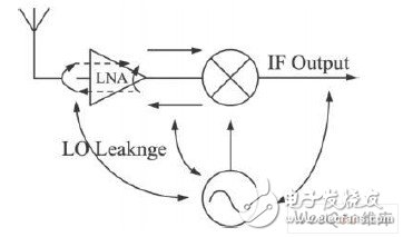
Figure 1 General receiver topology
To this end, the mixer designed in this paper uses the topology shown in Figure 2. This structure uses a local oscillator frequency multiplier circuit and a current multiplexing circuit to improve the isolation of the port and the conversion gain and linearity of the circuit. Since the LO signal is a differential input, in the case where the two differential tubes are identical, a virtual location of the AC signal is formed at node A, that is, the LO signal is short-circuited at point A, thereby improving the isolation of the mixer. At the same time, when the LO tube uses a short channel tube, the differential pair tube obtains the LO multiplication signal at node A, which will be analyzed in detail later. Therefore, the RF signal is mixed with the second harmonic signal of the LO signal and f IF = |fRF - 2fLO |. Using the local harmonics of the local oscillator will not cause LO signal leakage, and the frequency of the LO signal will be half that of the fundamental mixer, which greatly reduces the difficulty of the local oscillator design. The use of the inductor LE in the structure increases the amplitude of the second harmonic of the LO signal entering the mixing, which helps to increase the linearity and the noise figure. At the same time, the inductor acts as an enhancement of the push-pull path and expands the current. The dynamic range of the multiplexed circuit. The mixer's IF output is connected to the source follower as an output buffer.
Even harmonic mixer topology
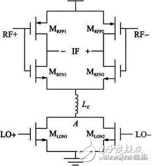
Figure 2 Even harmonic mixer topology.
1. 2 current multiplexing circuit analysis
The current multiplexing structure used at the RF input is shown in MRFP1 and MRFN 1 and MRFP2 and MRFN2 in Figure 2. The two-way structure is completely symmetrical. The transconductance of this structure is gm = gm p + gmn, where gmp is the transistors MRFP1 and MRFP2. Transconductance, gm n is the transconductance of transistors MRFN 1 and MRFN 2 . Therefore, the use of a current multiplexing structure increases the transconductance across the transconductance stage, thereby achieving high gain performance of the mixer.
According to the channel length effect, the cross-catheter current expression is:
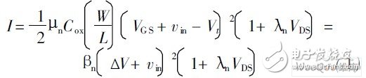
Here, n is the transconductance parameter, vin is the input signal, ! V = VG S - Vt is the overdrive voltage, n is the channel length modulation factor, and Vt is the threshold voltage. The output current can be obtained according to (1):
It can also be seen from equation (2) that the transconductance constituting the current multiplexing structure is the sum of the transconductances of the two transistors.
When the input signal is positive, the MRFN operates in the saturation region, and the MRFP operates in the cut-off region and is equivalent to the resistor RRFP. At this time, the entire current multiplexing structure is equivalent to an n-channel common-source amplifier. Similarly, when input When the signal is negative, the structure is equivalent to a p-channel common source amplifier. The current multiplexing structure constitutes a push-pull circuit and increases the dynamic range of the circuit, thereby improving the linearity of the circuit.
1. 3 frequency multiplier circuit
In order to further analyze the principle of the local oscillator signal multiplication, the inductive frequency multiplier circuit in the design mixer (Fig. 2) is given separately, as shown in Fig. 3. According to equation (1), the leakage currents ILON+ and ILON- of transistors MLON1 and MLON2 can be expressed as:
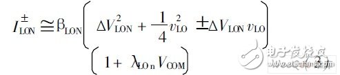
Here, vLO is the LO sinusoidal input signal, and aLO is the amplitude of the signal, ΔVLON = VLO - VTN is the overdrive voltage of MLON 1 and MLON 2. According to equation (3), the total current ICR flowing through the current multiplexing circuit and the frequency multiplying circuit is the sum of ILON+ and ILON-, that is,
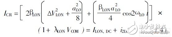
among them:
This signal is the 2nd harmonic signal of the LO. It can be seen from equation (4) that the LO multiplied signal i2LO is generated at the node VCOM while the fundamental frequency signal is cancelled. Assuming that the impedance of the inductor is ZLE = RLE + j2ωLOLE, the voltage Va at the mixing point can be expressed as:
Where, LE and RLE are the value of the inductor and the parasitic load, respectively. According to equation (5), due to the presence of the inductor, the voltage amplitude Va at the mixing is greater than VCOM, which improves the LO second harmonic signal entering the mixer. The power, which in turn increases the power of the wanted signal, helps to increase the linearity of the topology and also helps to reduce the noise figure.
Frequency multiplier circuit
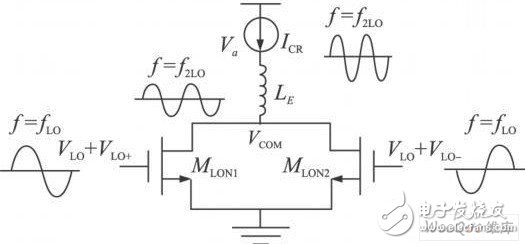
Figure 3 frequency multiplier circuit
Stainless Steel Bright Line,Stainless Steel Lock Wire,Inox Ss Stainless Steel Wire,Gasless Stainless Steel Mig Wire
ShenZhen Haofa Metal Precision Parts Technology Co., Ltd. , https://www.haofametals.com