0 Preface
High-power LED (light-emitting diode) devices are the core semiconductor lighting technology, which has become a research and development hotspot in recent years because it has more advantages than ordinary lighting technology. At present, ordinary light sources are mainly incandescent lamps, tungsten halogen lamps and fluorescent lamps. In theory, LEDs have the following advantages compared with these sources [1]. 1) High luminous efficiency, good monochromaticity of light, narrow spectrum, It can emit colored visible light directly without filtering. 2) Energy saving and low power consumption. Under the same lighting effect, LEDs consume one-eighth of the energy of incandescent bulbs and one-half of fluorescent tubes. 3) Long service life. LED lamps are small in size, light in weight, encapsulated in epoxy or silicone, and have high mechanical strength, resistance to vibration and shock. Theoretically, the average life of LEDs is 100,000 hours, which is dozens of times that of ordinary lamps. 4) Safe and environmentally friendly. LED is an all-solid-state illuminator with low calorific value and no heat radiation. It is a cold light source and contains no substances that may be harmful to health such as mercury and sodium. The waste can be recycled without pollution. Thanks to the above advantages, LEDs have begun to play a role in many applications. Typical applications are [2]: backlights for mobile phones and other LED displays, displays and signs, signal lights, etc.
For high-power LEDs, optical design and thermal management are two key factors for achieving high performance. Although the luminous efficiency of LEDs is theoretically high, the actual luminous efficiency of LEDs is still relatively low due to the lack of effective heat dissipation. The final luminous efficiency of most LED chips is only 10% to 20%, which means 80%~ 90% of the electricity is converted into heat. In general, this heat will greatly reduce the lighting efficiency. In addition to reducing the lighting efficiency, high temperatures will also cause changes in the color of the LED's illumination. In addition, higher LED operating temperatures will also cause the LED's lifetime to drop rapidly. In this regard, Narendran et al. [3] have confirmed through experiments that the lifetime of LEDs decreases exponentially with the increase in LED chip junction temperature. The above points indicate that the lower the operating temperature of the LED, the better. However, in practical applications, LEDs are often required to have high power and high packing density to achieve high brightness, which necessarily leads to a contradiction between power density and operating temperature, especially when the application conditions require the LED to operate at full load to achieve the desired brightness. This contradiction is more prominent. The above contradiction poses a challenge to the thermal management of high-brightness LEDs, and it urgently needs good heat-dissipation measures to solve the thermal problems of LEDs.
In order to effectively solve the problem of heat dissipation of LEDs, many researchers at home and abroad have carried out research on related thermal issues. In foreign countries, Arik et al. [4] used finite element method to carry out numerical simulation, solved the temperature distribution of LED chip and evaluated the influence of local high temperature on the active layer of the chip. Sano et al. [5] reported an ultra-bright LED module with excellent heat dissipation capability, which uses an aluminum substrate with excellent thermal conductivity to dissipate heat. Petroski [6] developed a new heat sink to achieve cooling of high-power LEDs that rely on natural convection for heat transfer. It uses a cylindrical structure surrounded by longitudinally distributed fins. This design can achieve heat dissipation isotropic. Chen et al. [7] use a silicon-processed thermo cooler (TE cooler) to cool high-power LEDs. Their test results show that the cooling method can effectively reduce the thermal resistance of high-power LEDs. Hsu et al. [8] reported a metal bonding method for LED packaging, which can achieve better heat dissipation and effectively reduce thermal resistance. Zhang et al. [9] used multi-walled carbon nanotubes and carbon black as thermal interface materials to encapsulate high-brightness LEDs. The test results show that this measure can effectively reduce the thermal resistance of LEDs. Acikalin et al. [10] used active cooling to reduce the LED operating temperature. They used a small piezoelectric fan to create forced convection. The test results show that the measure can reduce the heat source temperature by 37.4 ° C. The piezoelectric fan can be used as a competitive thermal management method for electronic devices and LED cooling.
In China, many researchers have also carried out research on LED thermal management. Wu Huiying et al. [11] used the finite element method to simulate the spatial temperature field distribution of 1W flip-chip high-power white LEDs. The simulation results are consistent with the measured temperature distribution. Based on the above numerical simulations, they also studied the relationship between chip size and junction temperature. The results show that: under certain luminous efficiency and package structure conditions, the design size and maximum capacity of the chip can be withstood due to the limitation of heat dissipation conditions. Power must be optimized. Yu Binhai et al. [12] analyzed the influence mechanism of chip substrate materials on the thermal characteristics of high-power LEDs. They established the relationship between the thickness and thermal conductivity of the flip-chip substrate bonding material and the thermal resistance of the bonding material. The three types of typical bonding materials were used as examples to calculate the thermal resistance at different thicknesses, and the flip-chip was obtained. The difference in the bonding material of the chip substrate has a great influence on the thermal resistance of the high-power LED. Chen Ying et al. [13] used a thermal impedance model to predict the temperature at the junction of the LED during operation and used it to guide the heat sink required to design a high-power LED source. By comparing with the actual situation, they verified the feasibility of the thermal impedance model and its guiding role in the design of thermal management of high-power LED light sources. Ma Chunlei et al. [14] described the principle, test device, measurement procedure and factors affecting the test results of high-power LED thermal resistance and junction temperature using dynamic electrical test methods. Their research shows that the method has the characteristics of simple test structure and high stability, and can be used as a standard test method for high-power LED thermal resistance and junction temperature. Wang Yutian et al. [15] analyzed the thermal characteristics of LEDs and derived engineering design formulas that reflect thermal characteristics and optical output power. Based on this formula, they calculated the optical power output of LEDs under pulse input conditions and analyzed the differences. Parameters such as pulse width, station-to-air ratio, etc. have an effect on optical power output and heat generation.
This paper proposes an active cooling scheme to achieve heat dissipation of high-power density LEDs. The solution uses a series of micro-spraying for heat exchange. The whole system is in closed form, which is circulated by a micropump drive system. Gases, liquids include water and even metal liquids. Both can be used as working medium. The micro-jet group relies on the good heat exchange effect of the impinging jet to bring heat from the LED into the cooling system to achieve heat dissipation. A large number of experiments have been carried out on the above system, and the experimental results show that it has better heat dissipation capability. In order to improve the current design, numerical experiments were carried out on the experimental system, and compared with the existing experimental results. The calculation results show that: The numerical model can be used as the means of the next stage analysis, and the experimental system currently designed needs to carry out parameter optimization.
1 closed micro-jet cooling system
Figure 1 shows a closed fluid cooling system based on a microjet stream set that is easily packaged with a cooled LED chip. In order to reduce system distortion and local stress problems between components, a special package structure and method is used to reduce the overall and local asymmetry of the cooling system and the chip.
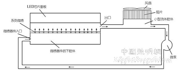
Figure 1 System schematic
Before the system is packaged and operated, a certain amount of fluid is injected into the system through the connection port, and then the joints are sealed to prevent fluid leakage. When the pump is energized, the fluid in the small fluid chamber enters the flow chamber through the inlet of the micro-injection device, and forms a strong jet through a series of nozzles under a certain pressure. The jet directly impacts the lower surface of the chip substrate or disturbs the fluid, resulting in a strong change. The thermal effect, the high heat flow generated by the LED chip is absorbed by the jet, the temperature drops sharply, the temperature of the fluid is increased due to the absorption of heat, and under the action of the pump, the warmed fluid flows out through the outlet of the micro-injection device, into the small fluid container, in the heat Under the action of the sink and the fan, the heat fluid and the environment exchange heat, causing the temperature to drop, and the low temperature fluid re-flows into the pump to start a new cycle.
Figure 2 shows a micro-jet group with a single-sided jet. In the figure, the fluid flows in from the inlet and passes through the upper wall of the micro-injection impact micro-injection device. The wall surface is made of a highly thermally conductive material, and the LED chip substrate is directly placed on the micro-injection device. In order to reduce the contact thermal resistance, a thermal paste is used between them. Or high thermal conductivity solder connected. After the low temperature jet contacts the high temperature LED chip pedestal, the temperature of the fluid rises, the temperature of the LED chip decreases, and the warmed fluid flows out of the outlet.
In order to meet the different applications of LEDs, the micro-injection device shown in Figure 2 can be modified into a variety of structures. The impinging jet cavity can be designed in the shape of a polyhedron or a cylindrical barrel, and the micro-spray is arranged on the inner surface of the polyhedron or cylindrical barrel, correspondingly, the LED The chips are placed on their outer surfaces, such a design that facilitates heat dissipation from multi-faceted LEDs.
The above cooling system adopts the impinging jet-jet heat exchange. Because the heat exchange coefficient of the impinging jet is large [16, 17] and the heat exchange effect is good, the high heat dissipation efficiency is its most significant advantage. Due to the multiple micro-spray, the LED substrate can achieve a uniform temperature distribution.
2 experimental system
Figure 3 is a physical diagram of the system depicted in Figure 1. The structural design and principle are basically the same as those of Figures 1 and 2. The heat sink and fan in Figure 3 are placed underneath the fluid container, as opposed to the description in Figure 1, but functionally. There is no significant difference between the effect and the effect. It is worth noting that the system shown in Figure 3 is an experimental device. In practical applications, the size of the micropump and the heat sink fan need to be reduced. Figure 4 is an experimental diagram of a 2 × 2 side-by-side arrangement of LED chips under the cooling of a micro-spray device. The surface temperature of the LED chip is measured by a Raytek non-contact infrared temperature tester. The temperature value is different from the temperature of the LED chip node. But it can intuitively reflect the temperature of the node. The main parameters and details in the above experiments are: The micropump is driven by the electromagnetic principle, and the input voltage can be adjusted to change the flow. By default, the micropump input voltage is 220 V AC and the flow rate is 10 mL/S. The design of a single microjet is 0.5 mm in diameter and the microjet is a 4x4 array. The working medium is water, heat sink and fan are very common products purchased directly in the computer market. In the experiment, the size of the small water tank is designed according to the size of the surface of the purchased heat sink. The experimental LED chip has a single size of 1 mm × 1 mm, a base size of 15 mm × 15 mm, and a distance of 3 mm between chips. Figure 5 shows the detailed dimensions of the test chipset and associated electrodes.

Figure 2 Single-spray micro-jet group
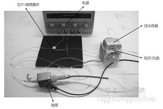
Figure 3 Experimental test system

Figure 4 LED chip surface temperature measurement
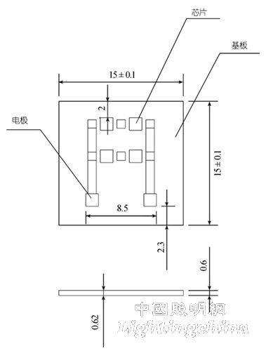
Figure 5 specific size of the test chipset
The specific dimensions of the experimental micro-spray device are shown in Figure 6. Since the size of the lower cavity is exactly the same as that of the upper cavity, Figure 6 only shows the size of the upper cavity. In Figure 6, the upper chamber has a length and width of 8 mm and a height of 6 mm. The outlet diameter on the upper chamber is 4 mm. The number of micro-jets inside the cavity is 16 and evenly arranged on an area of ​​8 mm × 8 mm, so that the pitch of each micro-spray is 1.6 mm. Since the LED chip substrate is directly disposed on the upper portion of the micro-spray cavity, the height of the micro-spray from the top plate is 6 mm. The lower chamber of the micro-jet device is completely identical to the upper chamber, and the inlet on the lower chamber has a diameter of 4 mm.
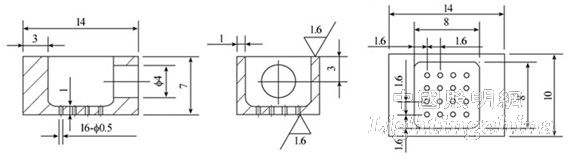
Figure 6 Dimensional drawing of the experimental micro-spray cavity
It is worth noting that all design dimensions of the experimental system are not specifically optimized for better performance, and further numerical simulation and optimization work is required.
3 experimental error analysis
The temperature is the main parameter of the experimental analysis. It is directly measured by the Raytek infrared thermometer. Since there are no other indirect measurement parameters, the error in the experiment is mainly the infrared thermometer error. The accuracy of the Raytek infrared thermometer is 98% accurate for 90% of the measured objects, which means the experimental error is about 2%.