Virtual instruments quickly occupied the market with their advantages of high cost performance and strong openness, and became a new economic growth point for measurement and control instruments. The most obvious sign of entering the information age is the penetration and popularization of information networks in various industries, among which Ethernet is the most typical. The Ethernet bus may replace other existing bus modes and become the preferred interface of the virtual instrument data acquisition system.
1 The overall design of the Ethernet interface 1.1 Ethernet interface design options There are usually three options for the design of the Ethernet interface: One is to use FPGA to achieve the description of the physical layer, network layer, access layer and transmission layer. It is difficult to implement the complex TCP / IP protocol on its own; the second is to implement network transmission based on the physical layer network controller and microprocessor. The advantage of this solution is that it has strong flexibility and can use different protocols for different systems. The protocol can be simplified: the third is to use a dedicated protocol processing chip to realize Ethernet data transmission. The hardware circuit of this solution is relatively simple, the development cycle is short, and there are more and more chips to choose from, and a variety of protocols are integrated. , Very easy to use.
This design uses a third interface scheme, which uses a dedicated TCP / IP protocol integrated chip, and the FPGA implements control of the protocol processing chip to achieve Ethernet data transmission. The protocol processing chip selects W3150A + which internally solidifies the TCP / IP protocol and cooperates with the physical layer chip RTL8201. The hardware circuit of this method is relatively simple, and can be realized by logic hardware, thereby making the system design simpler and more compact.
1.2 Introduction to Ethernet control chip W3150A + W3150A + is a TCP / IP protocol stack chip specially launched by WIZnet for Ethernet interconnection and embedded systems. W3150A + can implement protocols such as TCP, UDP, IP Ver.4, DHCP, ARP, and ICMP. At the same time, the network interface layer (including the MAC sublayer and DLC sublayer) can also be implemented in the chip. At the same time, it can also provide four-way network connection. Its 16KB dual-port RAM can be used as a data buffer and can support full-duplex mode. It also has a standard MD interface for easy connection to the physical layer interface chip. In addition, WIZnet also provides the Socket API package, which can accelerate the development of application programs.
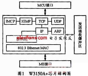

Figure 1 shows the block diagram of the W3150A + chip. As can be seen from Figure 1, W3150A + is mainly composed of 4 parts. The first part is the MCU interface. W3150A + provides direct bus interface, indirect bus interface and SPI bus interface. It is not only suitable for connecting with a bus like 8051 single chip microcomputer, but also very suitable for connecting with a controller with only IO port and no bus interface; the second part is the TCP / IP protocol stack. W3150A + has completely cured the protocols required from the MAC layer, network layer to the transport layer, so users do not need to understand the specific implementation methods and implementation codes of these protocols; the third part is the receive and send buffers, which communicate via Ethernet Data is exchanged through these buffers; the fourth part is the Ethernet physical layer interface (MII interface). W3150A + can be seamlessly connected with the physical layer chip RTL8201, thus achieving 10 / 100BaseT Ethernet physical interface.
The internal registers of W3150A + are divided into two memories and two types of registers. The two memories are used for input and output of data transmission. The two types of registers are general registers and port registers. Each type of register contains a large number of status word control registers. The following briefly introduces the more important status word control register.
Sn_MR: Port n mode register, this register is used to set the port options or protocol type;
Sn_CR: Port n command register, this register is used to set the port initialization, close, establish connection, disconnect, data transmission and command acceptance, etc .;
Sn_IR: Port n interrupt register, this register is used to display information such as establishing and terminating connection, receiving data, sending completion and time overflow;
Sn_PORT: Port number register of port n, this register can set the corresponding port number in TCP or UDP mode;
S_TX_FSR: Port n transmit memory remaining space register, this register is used to indicate the size of the transmit data space that the user can use, before sending data, the user must first check the size of the remaining space, and then control the number of bytes of transmitted data;
Sn_TX_RR: Port n transmit memory read pointer register. This register is used to indicate the current location of the transmit memory after the port is completed. When the SEND command is received in the command register of port n, it can be immediately sent out from the current Sn_TX_RR to Sn_TX_WR data. After the transmission is completed, the value of Sn_TX_RR automatically changes;
Sn_TX_WR: Port n transfer write pointer register, this register can indicate the address when writing data to the TX memory;
Sn_RX_RSR: Port n received data byte count register, this register is only the number of bytes received by the port receive data buffer, usually calculated from the value of Sn_TX_RR to Sn_TX_WR, after writing the RECV command to the port n command register The value will change automatically and can receive data from the remote peer;
Sn_RX_RD: Port n receive buffer read pointer register, this register is only the read address information after the port receiving process is completed.
There are 4 independent ports (Socket) inside W3150A +, and their status and control are mapped in the second to fifth register areas respectively. It is mainly used to control the working mode of the port (TCP server, TCP client, UDP or PPPOE, etc.), set the port number of the port, set the IP address and port number of the destination host of the port, and control the port receiving and sending data.
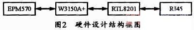
2 Hardware design of Ethernet interface The hardware design of this interface mainly includes the interface design of FPGA and W3150A +, the interface design of physical layer chip RTL8201 and W3150A + and the design of clock module and power module. The block diagram of its hardware design is shown in Figure 2.
2.1 Interface design between W3150A + and FPGA With the rapid development of semiconductor technology, the computing power, capacity and reliability of FPGA (Field Programmable Gate Array) have been greatly improved. It is becoming the new darling of digital circuits, digital signal processing and other fields with its advantages of highly flexible user on-site programming functions, repetitive rewritable functions, and high reliability.
Considering cost, practicality and power consumption, the FPGA chip selected for this design is EPM570GT100C4 of Altera's MAXII series. The MAXII series device is a non-volatile CPLD, using a 0.18μm manufacturing process, and contains 240 to 2210 logic cells and 8Kbits of non-volatile memory. It can provide fast, stable, and more quantity than other CPLDs. Multiple I / O pins.
There are three ways of interface between W3150A + and microprocessor chip: direct bus interface mode, indirect bus interface mode and SPI mode. Among them, the direct bus interface mode is suitable for the transmission of large amounts of data; the SPI mode has fewer interface connections, which is suitable for the case where the amount of data is not large and the transmission rate is relatively low; the data transmission performance in the indirect bus interface mode is between Between them. The system uses a direct bus interface mode to maximize the data transmission rate. Its concrete interface circuit is shown as in Fig. 3.
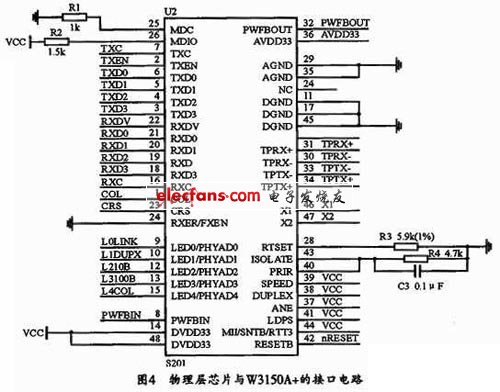
2.2 Interface design of the physical layer chip and W3150A + RTL8201BL is a single-port physical layer transceiver, it has only one MII / SNI (Media Independent Interface / Serial Network Interface) interface. Can be used to implement all 10 / 100M Ethernet physical layer functions, including physical layer coding sublayer (PCS), physical layer media connection equipment (PMA), twisted pair physical media related sublayer (TP ~ PMD), 10Base-Tx Codec and twisted pair media access unit (TPMAU). The PECL interface can support the connection of an external 100Base-FX fiber optic transceiver. This chip is manufactured using advanced CMOS technology, which can meet the needs of low voltage and low power consumption.
RTL8201BL and W3150A + can be connected through a standard MII interface, where pins RX_CLK, RXDV, RXD [0: 3] and COL are used for data reception, and TX_CLK, TXE, TXD [0: 3] are used for data transmission. The specific circuit diagram is shown in Figure 4.
  
55 Jack.China 4P4C RJ11 PCB Socket,Side Entry RJ11 Socket manufacturers, welcome RJ11 Jack Connector,2 Ports RJ11 Jack purchasers from worldwide to visit our site.
55 Modular Jack
4P4C RJ11 PCB Socket,Side Entry RJ11 Socket,RJ11 Jack Connector,2 Ports RJ11 Jack
ShenZhen Antenk Electronics Co,Ltd , https://www.antenk.com